In the dynamic world of electronics, Printed Circuit Boards (PCBs) power a wide range of devices. Although standard PCBs work well in many situations, some high-power and high-reliability applications demand extra robustness. In these scenarios, heavy copper PCBs rise to the challenge. They feature thicker copper layers for superior performance, durability, and reliability. In this comprehensive guide, you will discover the intricacies of heavy copper PCBs, learn about their advantages and applications, and explore how TriWin Circuits delivers these high-performance boards.
PCBs serve as the foundation for electronic systems, ensuring that components receive power and communication signals. While standard PCBs fit most consumer electronics, engineers often require specialized solutions for projects where high current flow or extreme environmental conditions prevail. Heavy copper PCBs excel in these demanding environments because they incorporate copper layers exceeding the thickness found in typical boards. Consequently, they offer greater current-carrying capacity, improved heat dissipation, and enhanced structural reliability. By understanding the full scope of heavy copper PCBs, you can make informed decisions for projects that call for sturdy, efficient, and long-lasting electronic assemblies.
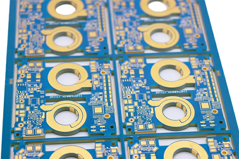
Composition and Structure
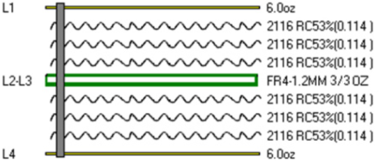
Copper Thickness
One of the most critical differences between standard and heavy copper PCBs lies in copper thickness. While a typical PCB may include 1 oz/ft² (about 35 micrometers) of copper, heavy copper PCBs often range from 2 oz/ft² to 10 oz/ft² or more. Thicker copper layers offer several key benefits:
- Higher Current Capacity: They handle substantial current without overheating, thereby reducing the risk of damage.
- Enhanced Thermal Conductivity: By dispersing heat more effectively, they help maintain stable operating conditions and improve component lifespans.
- Greater Durability: The additional copper thickness improves mechanical strength and allows these boards to perform reliably under stressful conditions.
Layers and Construction
Heavy copper PCBs may be single-sided, double-sided, or multi-layered, depending on the intended application. Engineers typically choose a specific stack-up to address the design’s voltage, current, and thermal requirements. Each layer includes:
- Core Material: Often FR-4 or another high-grade substrate that meets mechanical and electrical insulation needs.
- Copper Cladding: Laminated copper sheets of higher thickness that allow for heavy current flow and better heat conduction.
- Solder Mask and Silkscreen: Protective coatings that safeguard the copper from oxidation and help identify components during assembly.
By selecting superior core materials and applying the correct lamination processes, manufacturers deliver robust boards that maintain their performance in harsh environments.
Advantages of Heavy Copper PCBs
Enhanced Current Carrying Capacity
Heavy copper PCBs excel when used in power electronics because their thicker copper layers accommodate larger current loads. As a result, they prove indispensable in systems such as power supplies, battery chargers, and energy converters. Moreover, this advantage helps engineers maintain efficient circuit performance without sacrificing board integrity or component longevity.
Improved Thermal Performance
High temperatures pose a frequent threat to electronic components. Heavy copper PCBs, however, dissipate heat more effectively than standard boards. This characteristic is vital in applications where heat can accumulate, including motor controllers, industrial machinery, and automotive systems. When heat is managed efficiently, electronic assemblies can operate more reliably over a longer lifespan.
Durability and Reliability
Repeated thermal cycling, vibrations, and mechanical shocks can degrade standard PCBs over time. Heavy copper PCBs, on the other hand, stand up better to these challenges because of their robust construction. Engineers trust these boards in situations where consistent performance and minimal downtime are top priorities. As a result, industries that cannot afford failures rely on heavy copper PCBs to ensure stable operation.
Applications of Heavy Copper PCBs
High-Power Electronics
Heavy copper PCBs fulfill essential roles in high-power electronics, including power amplifiers and high-voltage converters. Designers depend on the boards’ superior current carrying capacity and heat dissipation to maintain efficiency under demanding conditions. Furthermore, their added resilience supports extended usage in power-hungry applications.
Industrial Machinery
The industrial sector demands equipment that can endure severe environments day in and day out. Heavy copper PCBs provide the ruggedness and reliability necessary for continuous operation, especially in machinery that produces significant vibration or heat. Consequently, factories integrate these boards into controllers and drive systems to minimize downtime.
Automotive Systems
Modern vehicles rely on countless electronic systems, from engine control units (ECUs) to power steering modules and advanced driver-assistance systems (ADAS). Many automotive designs incorporate heavy copper PCBs to ensure reliable performance under fluctuating temperatures, shocks, and extended operational hours. Because heavy copper boards handle these stresses well, they help maintain vehicle safety and efficiency.
LED Lighting
High-power LED lighting setups generate substantial heat, which calls for effective thermal management solutions. Heavy copper PCBs meet this need by dispersing heat quickly, thus preserving LED brightness and extending the life of the fixtures. Designers often place heavy copper boards at the core of advanced LED systems used in commercial and industrial lighting applications.
Manufacturing Process of Heavy Copper PCBs
Material Selection
Manufacturers achieve exceptional board performance by sourcing top-notch materials. At TriWin Circuits, for instance, we procure premium substrates and copper foils from reputable suppliers. We recognize that better input materials lead to more durable boards, so we remain committed to strict quality checks.
Fabrication Steps
- Design and Layout: Skilled engineers use advanced PCB design software to create optimized layouts that place components strategically and include proper spacing.
- Lamination: The manufacturing team laminates thick copper layers onto the core material under high temperature and pressure.
- Etching: We remove unneeded copper to form precise circuit traces with correct trace widths and clearance.
- Drilling and Plating: Engineers drill holes for components and vias before plating these holes with copper to establish robust inter-layer connections.
- Solder Mask Application: A solder mask is applied to protect copper surfaces and prevent accidental bridging during component soldering.
- Silkscreen Printing: Labels and orientation markers are printed to streamline component placement, maintenance, and troubleshooting.
- Quality Control: Our inspection specialists carefully check alignment, hole integrity, copper thickness, and continuity to confirm that each PCB meets design specifications.
Quality Control Measures
At TriWin Circuits, we use both automated and manual techniques to validate every PCB. Our certifications, including ISO9001, IATF16949, ISO14001, and UL, underscore our strict adherence to industry standards and best practices. By combining advanced inspection equipment and skilled personnel, we confirm each board’s performance before shipment.
Challenges and Considerations
Design Complexities
While heavy copper PCBs present many advantages, they also require cautious design due to the larger copper thickness. For example, engineers must decide on trace widths, clearances, and proper layering strategies to manage current flow and prevent complications like excessive heat buildup.
Cost Implications
Although heavy copper PCBs outperform standard boards in many respects, they tend to cost more because of the increased material usage and additional fabrication steps. Nonetheless, developers consider these higher costs a worthy trade-off when reliability and power handling are critical to the final product.
Handling and Assembly
Thicker copper layers make boards less flexible and slightly heavier. Therefore, assembly technicians must use proper handling techniques to avoid damage. In addition, manufacturers often employ specialized equipment or process adjustments to accommodate the board’s unique properties.
TriWin Circuits’ Expertise in Heavy Copper PCBs
Since its founding in 2015, TriWin Circuits has pursued excellence in manufacturing high-quality heavy copper PCBs. Our 10,000-square-meter factory in Huizhou, Guangdong Province, leverages advanced machinery and the expertise of more than 220 skilled engineers, experts, and technicians. With an annual production capacity of about 250,000 square meters, we handle large-scale or intricate PCB orders with confidence.
Comprehensive Quality Control
Our commitment to quality sets us apart. TriWin Circuits holds ISO9001, IATF16949, ISO14001, and UL certifications, which reflect our unwavering focus on customer satisfaction and precision manufacturing. We test every board exhaustively to eliminate defects and deliver products that achieve consistent performance under challenging conditions.
Versatile PCB Solutions
We understand that each project has unique requirements. As a result, we manufacture single-layer, double-layer, multi-layer, HDI, rigid-flex, and metal-based PCBs, including heavy copper boards. We rely on premium materials from Shengyi, ITEQ, and Kingboard, and we use high-quality Sun Ink to provide reliable solder masks. Our boards power applications in automotive lighting, BMS systems, medical equipment, and industrial control, among others.
Advanced Manufacturing Capabilities
We equip our production floor with leading technologies such as automated PTH lines, decontamination-plating-etching lines, LDI exposure machines, and screen printers. Consequently, we deliver precise prototypes and high-volume orders while maintaining consistent quality. Our technical investments, paired with our engineering know-how, guarantee that your heavy copper PCB projects meet or exceed your expectations.
Tips for Designing Heavy Copper PCBs
Consider Thermal Management
Effective thermal management ranks among the most important design considerations for heavy copper PCBs. By adding thermal vias, heat sinks, or copper fills around high-temperature components, you can guide excess heat away from sensitive areas.
Optimize Trace Widths and Spacing
Because heavy copper PCBs are thicker, electrical trace widths and spacing must align with the higher current capacities. Many designers rely on specialized software and industry guidelines, ensuring balanced trace layouts and minimized resistance.
Select Suitable Materials
High-quality substrates and copper foils can make or break a PCB’s reliability. Thus, check for certifications, material specs, and supplier reputations when choosing resources. TriWin Circuits prioritizes first-rate materials to achieve dependable results.
Implement Rigorous Testing
Comprehensive testing reduces the risk of failures in the field. By employing modern inspection equipment and verifying that all production stages meet or exceed standards, you set your product up for success.
Conclusion
Heavy copper PCBs offer unparalleled performance in high-power and high-reliability applications. Their thicker copper layers support greater current loads, dissipate heat efficiently, and endure harsh conditions better than standard boards. These attributes make them ideal for power electronics, industrial machinery, automotive systems, and LED lighting, among other demanding fields.
TriWin Circuits has cultivated deep expertise in delivering heavy copper PCBs since 2015. Our ISO9001, IATF16949, ISO14001, and UL certifications emphasize our commitment to stringent manufacturing standards and environmental practices. Moreover, our advanced equipment, premium materials, and highly skilled workforce enable us to produce boards that consistently meet complex specifications.Looking to upgrade your PCB designs or transition to heavy copper solutions? Contact TriWin Circuits today and explore how our dependable, high-reliability PCB solutions can elevate your electronic products. We strive to provide you with top-tier quality, excellent service, and innovative approaches that drive your projects to success.


