Introduction
Picture this: you’ve spent hours designing a perfect printed circuit board (PCB), only to find that it fails because a tiny component has decided to stand upright like a tombstone. This isn’t a scene from a sci-fi movie—it’s a real-world manufacturing defect called PCB tombstoning. Known for its quirky name and frustrating consequences, tombstoning is a common issue in electronics assembly that can lead to device malfunctions, costly repairs, and production delays. So, what exactly is PCB tombstoning, and how can you stop it from haunting your projects? In this article, we’ll explore its definition, causes, effects, and proven prevention strategies. Whether you’re a DIY enthusiast or a seasoned PCB manufacturer, this guide has something for you. Let’s get started.
What is PCB Tombstone?
PCB tombstoning is a soldering defect that occurs during the assembly of surface-mount technology (SMT) components. Imagine a small resistor or capacitor with one end soldered securely to the PCB while the other end lifts off its pad, standing vertically like a tombstone in a graveyard. This is tombstoning in action—also known as the Manhattan effect or drawbridge effect due to its upright appearance.
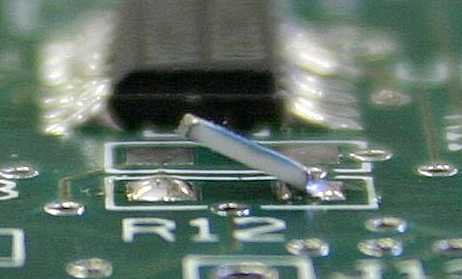
This defect typically strikes small, lightweight components like chip resistors and capacitors (e.g., 0402 or 0201 sizes) during the reflow soldering process. In reflow soldering, the PCB is heated in an oven to melt solder paste, bonding components to their pads. When something goes wrong—say, one pad solders before the other—the component gets pulled out of alignment, creating an open circuit. This means electricity can’t flow through the component as intended, potentially rendering the entire board useless.
Tombstoning isn’t just a random glitch; it’s a symptom of underlying issues in design, materials, or manufacturing. To tackle it, we first need to uncover why it happens. Let’s dig into the causes.
Causes of PCB Tombstoning
Tombstoning occurs when forces during soldering become unbalanced, lifting one end of a component while anchoring the other. Here are the primary reasons this defect rears its head:
1. Uneven Solder Wetting
Solder wetting is the process where molten solder spreads across a pad and bonds with a component’s lead. If the solder on one pad melts and wets faster than the other, it creates a lopsided pull—like a seesaw tipping too far to one side. This can happen due to:
- Inconsistent solder paste: Uneven application or poor-quality paste leads to differences in melting behavior.
- Temperature gradients: Nearby traces or components can heat one pad faster, causing premature wetting.
2. Thermal Imbalances
During reflow soldering, the PCB passes through an oven with carefully controlled temperature zones. If the heat isn’t uniform, solder on one pad might melt before the other, yanking the component upright. Common culprits include:
- Oven issues: Poor calibration or uneven airflow can create hot and cold spots.
- Board warpage: A bent PCB disrupts consistent heat distribution.
3. Design Flaws
Sometimes, the PCB’s layout sets the stage for tombstoning. Design-related triggers include:
- Mismatched pad sizes: A larger pad takes longer to heat, delaying solder melting and causing imbalance.
- Thermal sinks: Placing small components near large parts (like connectors) can siphon heat away unevenly.
- Pad spacing: If pads are too far apart, the component struggles to stay level during soldering.
4. Material Factors
The materials used in PCB assembly can also tip the scales toward tombstoning:
- Solder paste quality: Old, oxidized, or low-grade paste may not melt evenly.
- Component condition: Dirty or oxidized leads prevent proper solder adhesion.
- PCB surface finish: Finishes like Hot Air Solder Leveling (HASL) can lead to uneven solder thickness, increasing tombstoning risks.
These causes often overlap, making tombstoning a multifaceted challenge. But knowing what’s behind it is half the battle—next, let’s look at its real-world impact.
Effects of PCB Tombstoning
Tombstoning might sound like a minor quirk, but its effects ripple through both product performance and production workflows. Here’s why it matters:

1. Functional Impact
When a component tombstones, it breaks the circuit it’s meant to complete. This leads to:
- Open circuits: Electricity can’t flow, so the device either fails outright or behaves unpredictably.
- Reliability risks: In critical applications—like medical devices or automotive electronics—a tombstoned component could have catastrophic consequences.
For instance, a tombstoned capacitor in a power supply might cause flickering lights or sudden shutdowns, frustrating users and damaging reputations.
2. Production Costs
From a manufacturing standpoint, tombstoning is a profit-killer:
- Rework expenses: Fixing tombstoned components often requires manual soldering, driving up labor costs.
- Time delays: Defects spotted late in the process can stall production schedules.
- Scrap rates: Severely affected boards may need to be discarded entirely.
3. Modern Challenges
Tombstoning is especially relevant today due to industry trends:
- Miniaturization: Tiny components (e.g., 0201 packages) are lighter and more prone to lifting.
- Lead-free soldering: The shift to RoHS-compliant solders, which require higher temperatures and have trickier wetting properties, has made tombstoning more common.
In short, tombstoning isn’t just a technical annoyance—it’s a threat to quality, efficiency, and profitability. Fortunately, it’s preventable with the right approach.
How to Prevent PCB Tombstoning
Stopping tombstoning requires teamwork between designers, manufacturers, and quality control teams. Here are actionable strategies to keep your components flat and functional:
1. Design Tips
Good design lays the foundation for defect-free assembly:
- Symmetrical pads: Match pad sizes for each component to ensure even heating and wetting.
- Smart layouts: Keep small components away from large heat-absorbing parts or high-power traces.
- Orientation matters: Align components parallel to the reflow oven’s conveyor direction to minimize thermal gradients.
2. Manufacturing Adjustments
Precision in the assembly process is key:
- Thermal profiling: Use thermocouples to fine-tune reflow oven settings, ensuring uniform heat across the board.
- Solder paste precision: Apply paste evenly with well-designed stencils and store it properly to maintain quality.
- Placement accuracy: Calibrate pick-and-place machines to center components perfectly on their pads.
3. Quality Control
Catch issues before they escalate:
- Inspection tools: Use Automated Optical Inspection (AOI) or X-ray systems to spot tombstoning early.
- Material checks: Verify solder paste freshness and component lead quality before assembly.
- Process monitoring: Regularly test oven performance and solder paste viscosity to maintain consistency.
At TriWin PCB, we’ve mastered these techniques and more. Our cutting-edge equipment—like LDI exposure machines and automated PTH lines—delivers precision that minimizes defects like tombstoning. Combined with rigorous testing (e.g., flying probe and impedance checks), we ensure your boards meet the highest standards. Partner with us, and you’re choosing reliability over rework.
Conclusion
PCB tombstoning may look like a small defect, but its potential to disrupt functionality and inflate costs makes it a big deal. By understanding its causes—uneven solder wetting, thermal imbalances, design flaws, and material hiccups—you can take control. Better still, with proactive prevention—through thoughtful design, precise manufacturing, and thorough quality checks—you can stop tombstoning before it starts.
In an era of shrinking components and stricter standards, mastering defects like tombstoning is essential for producing reliable electronics. Whether you’re building a one-off prototype or ramping up for mass production, the stakes are too high to ignore.
Struggling with tombstoning or ready to elevate your PCB game? Contact TriWin PCB today. We’re here to turn your ideas into flawless, high-performing boards—tombstone-free.
FAQs
Q: Why is tombstoning more common with smaller components?
A: Small components (like 0402 or 0201 sizes) are lighter, so they’re more easily pulled upright by uneven soldering forces.
Q: Can tombstoning be repaired?
A: Yes, but it’s tedious. Manual rework with a soldering iron can fix it, though this adds time and expense.
Q: Does lead-free solder increase tombstoning risks?
A: Absolutely. Lead-free solders need higher temperatures and wet differently, making imbalances more likely.
Q: How do I spot tombstoning?
A: Look for components standing upright on one end. Testing will also reveal an open circuit.
Q: Does PCB color play a role in tombstoning?
A: No, color is cosmetic and doesn’t affect soldering or defect rates.


