Introduction
In the rapidly evolving world of electronics, High-Density Interconnect (HDI) PCBs play a crucial role in modern devices. Designers and manufacturers use these advanced circuit boards to meet the increasing demand for smaller, faster, and more efficient electronic products. Understanding HDI PCBs is essential for anyone involved in electronics design and manufacturing.
Definition and Characteristics of HDI PCB
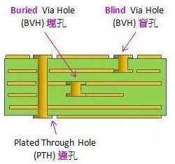
HDI PCBs are characterized by their high wiring density, which is achieved through the use of micro vias, blind and buried vias, and fine lines and spaces. Unlike traditional PCBs, HDI boards allow for more complex and compact designs, making them ideal for applications where space is at a premium. The use of micro vias, which are smaller than conventional vias, enables designers to create more intricate interconnections between layers.
Types of HDI PCBs
There are several types of HDI PCBs, each suited to different applications:
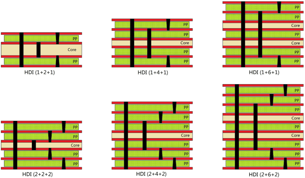
- 1+N+1: This basic structure includes a single build-up layer on each side of a core.
- 2+N+2: More complex, with two build-up layers on each side, allowing for even greater interconnect density.
- Via Types: HDI PCBs utilize various via types, including micro vias, blind vias (connecting outer layers to inner layers), buried vias (connecting inner layers only), and stacked or staggered vias for multi-layer connections.
Advantages of HDI PCBs
HDI PCBs offer numerous advantages:
- Enhanced Performance: The high density of interconnections improves signal integrity and reduces transmission losses.
- Space-saving: Their compact design allows for smaller, lighter devices without sacrificing functionality.
- Versatile Applications: Various industries, including automotive, aerospace, medical, and consumer electronics, use HDI technology to support complex circuitry in limited space.
Manufacturing Process of HDI PCBs
The manufacturing of HDI PCBs involves several advanced processes:
- Lamination: Manufacturers laminate multiple layers together to form the board’s structure.
- Laser Drilling: Technicians use precision laser technology to drill microvias, which enables high-density connections.
- Challenges: Designing and fabricating HDI PCBs requires careful consideration of thermal management, material selection, and process control to ensure reliability and performance.
Applications of HDI PCBs
HDI PCBs are integral to many modern devices:
- Consumer Electronics: Smartphones, tablets, and laptops rely on HDI technology for their compact and powerful designs.
- Automotive Electronics: Advanced driver-assistance systems (ADAS) and infotainment systems benefit from HDI’s high performance and reliability.
- Medical Devices: Miniaturized medical instruments and wearable devices utilize HDI PCBs for their precision and efficiency.
Conclusion
HDI PCBs represent a significant advancement in PCB technology, offering unparalleled performance and versatility. As electronic devices continue to shrink in size while increasing in functionality, the demand for HDI PCBs is expected to grow. Understanding the benefits and applications of HDI technology is crucial for staying competitive in the electronics industry.
By leveraging the capabilities of HDI PCBs, manufacturers can create innovative products that meet the ever-evolving needs of consumers and industries alike.


