Introduction: The Unsung Heroes of Modern Electronics
Printed Circuit Boards (PCBs) are the fundamental backbone of modern electronic devices. As electronics demand greater miniaturization and higher performance, multilayer PCB designs have become essential. This evolution created a critical need: connecting electrical signals and power paths vertically between these stacked layers.
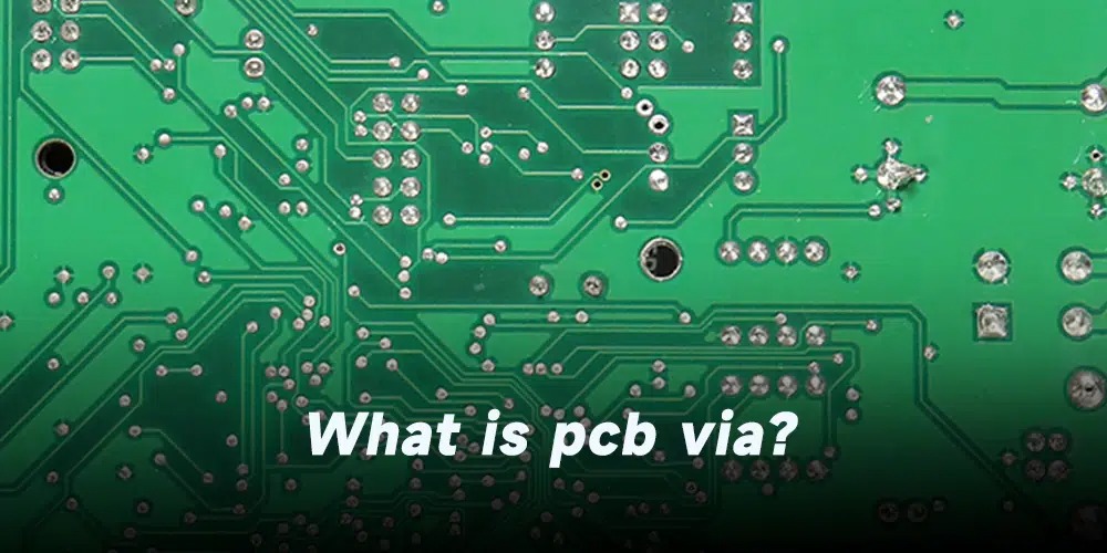
This is where vias become indispensable. A via, short for Vertical Interconnect Access, is a small, conductive pathway that bridges different layers of a PCB. These plated holes enable three-dimensional circuit routing, maximizing routing density and minimizing overall board size. Without vias, the intricate, multi-layered designs found in smartphones, laptops, and smartwatches would be impossible.
Beyond simple connectivity, vias are crucial for signal integrity, efficient power delivery, and effective thermal management in high-performance, high-density, and high-frequency applications. Even minor discontinuities introduced by vias can significantly impact device performance as operating frequencies and data rates climb. This article will explore the fundamentals of PCB vias, their diverse types, manufacturing processes, critical design considerations, and their vital role in advanced electronic designs.
1. What Exactly is a PCB Via? Unpacking the Fundamentals
To understand vias, we must grasp their basic definition and anatomical components.
1.1. Defining the PCB Via: Purpose and Basic Structure
A PCB via is a small, conductive, copper-plated hole drilled or laser-cut through PCB laminates. Its primary function is to establish electrical connections between two or more adjoining layers. This vertical connectivity is essential for complex multi-layered designs, allowing signals and power to flow between different planes and traces, thereby maximizing routing density and minimizing board footprint.
Unlike general non-plated holes (NPTH) used for mechanical purposes, a via is specifically engineered for electrical connection, featuring a conductive plating along its barrel and an annular ring at its ends. This annular ring, a copper ring around the drilled hole, is critical for a reliable electrical connection to traces or planes.
1.2. Anatomy of a Via: Barrel, Pad (Annular Ring), and Antipad
A via’s core components are:
- Barrel: The conductive copper tube lining the drilled hole, acting as the primary conduit for electrical signals or power between layers. Its integrity and thickness are vital for current-carrying capacity and reliability.
- Pad (Annular Ring): The circular copper area surrounding the drilled hole on each connected layer. It’s the crucial connection point between the via barrel and traces, planes, or component pads. Proper sizing ensures a reliable and durable connection, improving manufacturing yield.
- Antipad: A void or gap in copper layers where the via is not intended to connect. It prevents unwanted electrical contact and helps control the via’s parasitic capacitance, crucial for impedance control in high-frequency designs.
The precise design of these components directly dictates the via’s electrical performance and manufacturability.
2. Diverse Types of PCB Vias: Tailored for Every Design Challenge
Various via types have evolved to meet specific design challenges, performance requirements, and manufacturing capabilities.
2.1. Through-Hole Vias: The Traditional Workhorse
Through-hole vias are the most common type, extending completely from the top to the bottom layer, created by mechanical drilling. They are robust, cost-effective, and offer good heat dissipation. However, they consume significant board space and can introduce signal reflection issues (via stub effect) in high-speed applications.
2.2. Blind Vias: Connecting Outer to Inner Layers
Blind vias connect an outer layer to one or more internal layers without penetrating the entire board, visible from only one side. They are crucial for High-Density Interconnect (HDI) boards, enhancing routing density and improving signal integrity with shorter paths. Manufacturing is more complex and costly, often requiring laser drilling and sequential lamination.
2.3. Buried Vias: Internal Layer Interconnects
Buried vias are entirely enclosed within the PCB, connecting two or more internal layers without reaching either outer surface. Ideal for dense, multilayer designs, they maximize board space, reduce PCB size, and aid in Electromagnetic Interference (EMI) control. They are the most expensive and complex to manufacture, requiring multiple lamination steps.
2.4. Microvias: Enabling High-Density Interconnect (HDI)
Microvias are exceptionally small vias (typically under 150 micrometers), primarily created using advanced laser drilling. Essential for HDI PCBs (smartphones, wearables), they optimize routing space, enable finer line pitches, and enhance signal integrity due to shorter paths and reduced parasitic capacitance. Their intricate production makes them considerably more costly.
2.5. Via-in-Pad Technology: Direct Component Connectivity
Via-in-pad places the via directly within a component’s solder pad, often for fine-pitch components like BGAs. This shortens trace lengths, benefiting high-frequency signals, and allows greater routing density. The via must be filled and capped to prevent solder wicking, adding manufacturing complexity and cost.
2.6. Specialized Via Configurations for Enhanced Performance
- Thermal Vias: Placed under high-power components to efficiently conduct heat away, maintaining optimal operating temperatures.
- Tented & Filled Vias: Tented vias are covered with solder mask for protection. Filled vias are filled with epoxy or conductive paste for structural integrity, preventing solder wicking, or enhancing heat transfer.
- Stitching Vias: Numerous small vias between power/ground planes or along RF traces to improve power delivery, enhance signal strength, provide robust grounding, and control EMI.
- Via Fencing: A continuous barrier of grounded vias around sensitive areas to create an electromagnetic shield, blocking noise.
- Star Grounding: All ground paths connect to a single central via to prevent ground loops and ensure a stable ground reference.
- Stacked & Staggered Vias: Stacked vias are vertically aligned, while staggered vias are offset. Both optimize space in advanced packaging, with stacked vias requiring higher precision and cost.
- Skip Vias: Connect non-adjacent layers, bypassing intervening ones to optimize signal integrity and reduce EMI.
- Boomerang Vias: A technique used in high-speed designs to mitigate via stub issues near edge connectors by ensuring the signal travels the full via length.
The choice of via type involves balancing performance advantages against manufacturing challenges and cost implications.
Table 1: Comparison of Common PCB Via Types
| Via Type | Description/Characteristics | Typical Applications | Key Advantages | Key Disadvantages | Primary Manufacturing Method |
| Through-Hole | Extends completely from top to bottom layer; mechanically drilled. | General purpose, mechanical support, high-current connections. | Cost-effective, easy to manufacture, good heat dissipation. | Consumes significant board space, can cause signal reflection (stub effect) in high-speed designs. | Mechanical Drilling |
| Blind Via | Connects an outer layer to one or more internal layers; visible from one side. | High-Density Interconnect (HDI) boards, space-constrained designs. | Increases routing density, improves signal integrity (shorter path), optimizes space. | More complex and costly to produce, requires sequential lamination. | Mechanical or Laser Drilling |
| Buried Via | Connects internal layers only; not visible from outer surfaces. | Dense, multilayer designs, high-signal integrity applications, EMI control. | Maximizes board space utilization, enhances dense routing, aids EMI control. | Most expensive and complex to manufacture, difficult to inspect/troubleshoot. | Mechanical or Laser Drilling, Multiple Lamination Steps |
| Microvia | Very small diameter (typically <150 µm); laser drilled. | HDI PCBs (smartphones, wearables), high-speed circuits, fine-pitch BGAs. | Optimizes routing space, enables finer pitches, excellent signal integrity (reduced parasitics). | Costlier due to intricate laser drilling process. | Laser Drilling |
| Via-in-Pad | Placed directly within a component’s solder pad; filled and capped. | Fine-pitch components (BGAs, QFNs), high-frequency signals, tight spaces. | Shortens trace lengths, improves signal quality, reduces solder bridging, increases routing density. | Requires filling and capping, adds manufacturing complexity and cost. | Mechanical or Laser Drilling, Filling & Capping |
3. The Manufacturing Journey of a PCB Via
The creation of functional vias involves precise manufacturing steps that directly influence board quality.
3.1. Drilling Techniques: Mechanical vs. Laser Precision
- Mechanical Drilling: Traditional, affordable, suitable for regular-sized vias. Limitations include smaller holes and potential mechanical stress.
- Laser Drilling: Advanced, uses focused laser beams for microvias and extreme precision in HDI boards. More expensive but offers superior accuracy and cleaner holes.
3.2. Plating and Filling Processes: Ensuring Conductivity and Reliability
After drilling, holes are transformed into functional vias:
- Chemical Treatment and Electroplating: Holes are chemically prepared, then electroplated with copper to form the via barrel. This ensures robust electrical connections, adequate current-carrying capacity, and durability.
- Via Filling and Capping: For certain vias (e.g., via-in-pad), holes are filled with non-conductive epoxy or conductive paste, then capped (plated over) to create a flat, solderable surface.
- Via Tenting: Covering via openings with solder mask insulates the copper, prevents contaminants, and protects against shorts, improving reliability and appearance.
These manufacturing processes are practical constraints that actively shape design choices, emphasizing the need to integrate manufacturing considerations early in design.
4. Critical Design Considerations for Optimal Via Performance
Meticulous via design is crucial for PCB performance and reliability.
4.1. Strategic Selection and Placement of Via Types
Choosing the right via type is fundamental, based on application requirements like speed, density, power, and cost. Smaller vias, like microvias, increase routing density in compact designs. Strategic placement optimizes signal integrity, minimizes crosstalk, and reduces EMI, especially near high-frequency components.
4.2. Mastering Via Size, Aspect Ratio, and Annular Ring Design
- Via Size & Aspect Ratio: The ratio of via depth to diameter impacts manufacturability and plating quality. High aspect ratios risk drilling issues and uneven plating, compromising reliability. Lower aspect ratios reduce parasitic inductance, benefiting high-speed applications.
- Annular Ring Requirements: An adequately sized annular ring (copper pad around the hole) is essential for reliable, long-lasting connections. Too small, and it can lead to drill breakout, poor conductivity, or open circuits.
4.3. Adhering to Clearance and Spacing Guidelines
Maintaining proper clearance and spacing between vias, traces, and components ensures reliable signal transmission, reduces crosstalk, and enhances overall PCB performance. Insufficient spacing, especially in high-frequency designs, can cause impedance mismatches and signal degradation.
4.4. Mitigating Signal Integrity Issues: The Challenge of Via Stubs and Back Drilling
In high-speed digital and RF designs, the “via stub” (unused portion of a through-hole via) can cause signal reflections and attenuation, acting as a “low pass filter” at high frequencies (e.g., 32 Gbps and above).
Techniques to minimize or eliminate stubs include:
- Back Drilling: Mechanically drilling away the unused via stub from the bottom of the PCB, reducing parasitic capacitance and inductance. This adds cost and carries a risk of drilling too deep.
- Using Blind or Buried Vias: These types inherently minimize stubs by connecting only necessary layers.
- Via-in-Pad: Minimizes stub length by placing the via directly under the component pad.
- Boomerang Vias: Routes signals to ensure they travel the full via length, eliminating problematic stubs.
4.5. The Role of Via Plating Thickness
Thicker copper plating within the via barrel increases current carrying capacity and durability, crucial for power and ground vias. While beneficial, it adds manufacturing cost and time.
4.6. Design for Manufacturability (DFM) and Collaboration with PCB Manufacturers
Comprehensive Design for Manufacturability (DFM) checks analyze designs for potential via-related manufacturing issues (e.g., aspect ratio violations, insufficient annular rings, tight spacing). Proactive DFM saves time and avoids costly errors. Close collaboration with the PCB manufacturer is essential to align via design with their specific capabilities and design rule recommendations, optimizing yield and reducing production costs.
Table 2: Key Design Considerations for PCB Vias
| Consideration | Key Guideline/Impact | Why it Matters (Impact on Performance, Manufacturability, Cost, Reliability) |
| Via Type Selection | Choose based on application (speed, density, power) and cost. Smaller vias for higher density. | Directly impacts routing density, signal integrity, and overall board cost. |
| Strategic Placement | Place away from critical components/traces; near high-frequency components for EMI. | Optimizes signal integrity, minimizes crosstalk, reduces EMI, and influences thermal performance. |
| Via Size & Aspect Ratio | Maintain appropriate aspect ratio (depth/diameter) for manufacturability. Lower ratio for signal performance. | Affects drilling success, plating quality, parasitic inductance, and board reliability. |
| Annular Ring | Ensure sufficiently large copper pad around via hole. | Critical for reliable, long-lasting connections, prevents drill breakout, impacts manufacturing yield. |
| Clearance & Spacing | Adhere to adequate spacing between vias, traces, components. | Ensures reliable signal transmission, reduces crosstalk, prevents impedance mismatches. |
| Via Stubs | Minimize or eliminate unused via length (stubs) in high-speed/RF designs. | Prevents signal reflections, reduces insertion loss, maintains signal integrity. |
| Plating Thickness | Thicker plating for higher current capacity and durability (power/ground vias). | Impacts current carrying capacity, durability, manufacturing cost, and board density. |
| Design for Manufacturability (DFM) | Conduct checks for manufacturing issues; collaborate with manufacturer. | Proactively identifies and addresses issues, saves time/cost, ensures manufacturability and yield. |
5. Vias in High-Speed and Radio Frequency (RF) Design
At high frequencies, vias are not simple conductors; their physical characteristics introduce complex electrical phenomena that can degrade signal quality.
5.1. Understanding Parasitic Effects: Capacitance and Inductance
At high frequencies (e.g., 32 Gbps and above, or GHz range), vias introduce significant parasitic capacitance and inductance, acting as transmission line discontinuities. Parasitic capacitance causes unintended coupling and negative reflections from via stubs. Parasitic inductance arises from the via structure itself; minimizing via diameters (e.g., 0.2-0.4 mm) helps reduce this.
5.2. Achieving Impedance Control and Matching
For optimal signal integrity, via impedance must match transmission line impedance (typically 50 Ω). Mismatches lead to reflections and signal degradation. Strategies include adjusting antipad size, using stitching vias for channels above 5 GHz, minimizing via diameters, and ensuring reliable ground return paths.
5.3. Managing Signal Loss and Reflections
High-frequency signals are highly susceptible to loss and reflections from vias. Multiple vias can cause severe attenuation, acting as a “low pass filter.” Key strategies include stub minimization (back drilling, blind/buried vias, via-in-pad, boomerang vias), via stitching and fencing for high-frequency isolation, keeping transitions electrically short, and selecting RF PCB materials with lower dielectric constants.
5.4. Thermal Management in High-Density RF Boards
Effective thermal management is crucial for high-density RF boards. Thermal vias are integrated under heat-generating components to dissipate heat into internal copper planes or heat sinks. Proper thermal relief patterns and increased plated wall thickness (e.g., 100 µm) further enhance heat transfer.
6. Quality Control and Common Via Defects
Ensuring via quality is paramount for PCB performance and longevity.
6.1. Essential Testing Methods for Via Quality
- Automated Optical Inspection (AOI): Identifies visual defects like missing pads or shorts.
- X-ray Inspection: Crucial for blind and buried vias, checking internal plating and alignment.
- Time-Domain Reflectometry (TDR): Characterizes via impedance, detecting discontinuities and reflections in high-speed designs.
- HiPot Testing: Applies high voltage to check insulation breakdown and dielectric strength.
- Cross-section Analysis: Destructive test providing detailed internal views of via structure, plating quality, and dimple measurement.
6.2. Identifying and Addressing Common Via Defects
Common defects include:
- Voids: Empty spots in copper plating, compromising conductivity and current capacity.
- Barrel Fatigue/Cracks: Cracks in copper plating from thermal cycling or stress, leading to intermittent connections.
- Misalignment (Drill Breakout): Drilled hole not aligning with the annular ring, causing weak connections or open circuits.
- Solder Wicking: Solder flowing into an improperly filled/capped via-in-pad during reflow, leading to poor solder joints.
Mitigation involves adhering to aspect ratios, using thermal relief pads, respecting manufacturer limits, and proactive DFM checks with manufacturers.
7. Applications of PCB Vias Across Industries
Vias are integral to electronic devices across virtually every sector:
- Consumer Electronics: Fundamental for compact devices like smartphones, laptops, and wearables, enabling high-density routing and signal integrity. Also crucial for entertainment systems and home appliances.
- Medical Devices: Essential for small, reliable PCBs in pacemakers, infusion pumps, and medical lighting, where precision is paramount.
- Industrial Equipment: Power critical systems like power inverters, solar equipment, and control systems. Growing demand with industrial IoT and robotics.
- Automotive Sector: Integral to engine management, fuel regulators, blind spot monitoring, and autonomous driving systems, requiring high-reliability vias for harsh conditions.
- Aerospace & Maritime: Crucial for communication, navigation, and monitoring equipment in planes, satellites, and marine vessels, demanding PCBs that withstand extreme environments.
- LED Lighting, Computer Peripherals, Safety & Security: Vias are foundational across these and other electronic product developments.
Continuous innovation in via technology, including embedded components and 3D printed vias, promises even more compact, efficient, and complex electronic designs.
Conclusion: The Future of Connectivity
The PCB via has evolved from a simple conductive hole into a sophisticated and indispensable component in modern electronics. Its role has expanded significantly to meet the complex demands of high-density, high-speed, and high-frequency designs.
The diverse via types, from through-hole to advanced microvias, highlight the continuous engineering challenge of balancing performance optimization with manufacturing feasibility and cost. Each type offers distinct advantages, such as increased routing density, improved signal integrity, or enhanced thermal management, often with trade-offs in complexity and cost.
The critical impact of vias on signal integrity in high-speed and RF applications, particularly concerning parasitic effects and via stubs, necessitates meticulous design considerations. Techniques like back drilling, via stitching, and careful impedance matching are essential for reliable signal transmission. The intricate manufacturing journey of a via underscores the crucial role of Design for Manufacturability (DFM) and close collaboration with PCB manufacturers to bridge theoretical design ideals with real-world production capabilities.
As electronic devices continue to miniaturize and accelerate, the importance of vias will only grow. Future advancements in via technology promise to unlock new possibilities for compactness, efficiency, and functionality. A deep understanding of via fundamentals, types, design considerations, manufacturing processes, and quality control is essential for engineers and designers to push the boundaries of electronic innovation and ensure the continued reliability and performance of the next generation of electronic products.
At Triwin, we understand the critical role of every detail, including the precise design and manufacturing of vias, in achieving high-reliability PCBs. Our expertise in producing a wide array of advanced PCBs, including HDI, high-frequency, and metal base boards, is built upon state-of-the-art manufacturing capabilities and rigorous quality assurance processes. We are committed to delivering an “All-Around PCB Supplies Solution,” ensuring that every via on your board contributes to optimal performance and long-term reliability.


