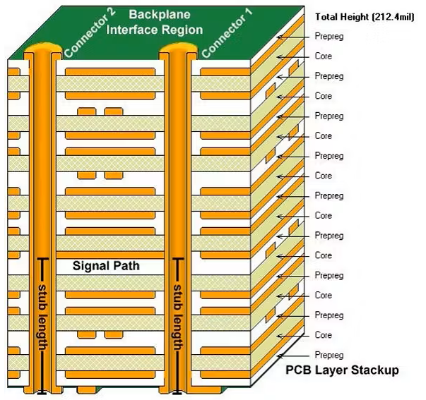
The backplane is a PCB board with many slots, which contains few (or no) active circuits, usually one or several of these slots are used for switching or core computing, while the rest of the slots can flexibly expand different interfaces or functions, and each slot through the backplane to achieve dense high-speed interconnection.
Basic parameters (Customizable):
| Layers: | 18 Layers |
| Material: | S1000-2M |
| Finish board thickness: | 5.4mm |
| Finish copper thickness: | 1 oz |
| Surface treatment: | ENIG |
| Solder mask: | Green |
| Notes: | UL/ISO/SGS certification. |
 ||
||
What is backplane PCB?
The backplane is a PCB board with many slots, which contains few (or no) active circuits, usually one or several of these slots are used for switching or core computing, while the rest of the slots can flexibly expand different interfaces or functions, and each slot through the backplane to achieve dense high-speed interconnection. In the optical backplane technology is not fully mature today, the transmission technology of electrical signals is still the mainstream backplane implementation scheme. A typical backplane will use more than 20 layers of PCB laminated structure and carry thousands of pairs of high-speed differential wiring.
PCB design Where multiple boards need to be connected into a larger system and provide interconnections between them, a backplane may be used to arrange and cascade these boards. The backplane is a premium board that borrows certain elements from high-speed design, mechanical design, high voltage/high current design and even RF design. These boards are commonly used in mission-critical defense systems, telecommunications systems, and data centers.
Features:
The backplane is used to support the many kinds of Individual PCB boards. A circuit board for interconnecting smaller boards. It is thicker and heavier than regular PCB boards.
The backplane is basically a connector with few or no components.
The backplane can be used to connect multiple devices, modules, or boards together for high-speed data transmission, signal transmission, and control functions. Backplanes typically have multiple connectors that can be plugged into different modules or boards and connected via high-speed signal cables or optical fibers. To give an easy to understand example: the backplane is like the motherboard of our computer, the graphics card, memory, hard disk, CPU are plugged into the motherboard. The backboard acts like a motherboard.
Compare Individual PCB boards and backplanes:
Individual board: A functional module consisting of a Individual PCB board (backplane connection is not necessarily required, such as cable jumper or laminated connection).
Backplane: A special board used to connect individual boards to form a complete box system.
Backplanes may have higher technical requirements (in terms of power and speed, etc.) than boards. The technical specifications of the backplane directly affect the performance of the whole system.
Application:
Backplanes are widely used in computer, communication equipment, network equipment, data center servers, industrial automation control, military aviation and other fields.
Please send us your PCB data (include gerber and specs), and quantity you need, as well as the mode of delivery, we will provide price to you ASAP, our Email address please see “Contact us”page.
Please send us your PCB data (include gerber and specs), together with your purchase order (PO),our Email address please see “Contact us”page, we will provide EQ (engineering query) (if have) to you ASAP, after all engineering questions are solved, we will start production and ship to you within your required delivery date.
Trace width/space: 0.075/0.075mm min., 0.1/0.1mm generally for 1 oz copper. Via size: 0.15mm mechanical drill, Board thickness: 0.4mm for rigid PCBs.
Yes, we are professional Aluminum base PCB supplier, we also produce Copper base PCB, FR4 PCB, such as double sides, multilayer, HDI, Flex-rigid, Flex, and so on.
Yes, we could panelized your different single PCBs together in one panel when production, and rout panel into individual PCBs before delivery.
RS 274x format is the best and most common gerber format, of course, files designed by PROTEL99SE, Altium Designer, PADS are also OK for us.
Generally speaking, 2-3 working days for sample, 6-7working days for mass production. Of course, delivery date concerned with the level of difficulty, such as layers and PCB type, more process need more time.
ENIG (Immersion gold), Selective hard gold, HASL lead free, OSP, Immersion tin, Immersion silver, ENEPIG, etc.
S1141, S1000H, S1000-2, S1155, S1165, KB6060, KB6165, IT158C, IT180A, 370HR, VT-47, FR408、FR408HR、IS410、FR406, EM827, TU 752, Rogers 4003, Rogers 4350, etc.
If your PCB need other special brand material, we could manage to purchase it for you.
Your Trusted Partner for Reliable PCB Solutions.

Copyright © 2024, TriWin P.C.B. Co.,Ltd All rights reserved