Introduction
Printed Circuit Boards (PCBs) are critical components in modern electronic devices, providing the foundation for electrical connections between various components. However, one of the challenges faced in PCB manufacturing is warpage, specifically in the form of bow and twist. These deformations can significantly impact the performance and reliability of PCBs.
In this article, we will explore what PCB bow and twist are, their causes, industry standards, prevention strategies, and solutions for existing issues.
As a professional PCB manufacturer established in 2015, TriWin is committed to producing high-quality PCBs that meet stringent standards for flatness and reliability. With over 220 experienced experts and a production capacity of approximately 250,000 square meters annually, we ensure that our products meet the needs of our clients across various industries.
1. Understanding PCB Bow and Twist
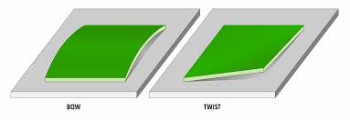
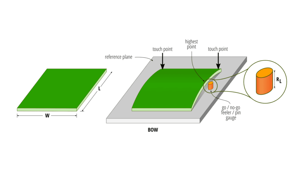
1.1 What is PCB Bow?
PCB bow refers to a condition where the board is not flat but instead has a curvature along its length or width. This warpage can lead to difficulties during assembly processes, such as soldering or component placement, potentially resulting in poor electrical connections or mechanical stress on components.
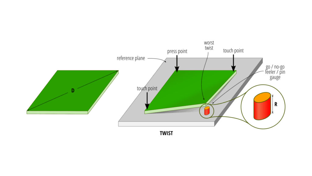
1.2 What is PCB Twist?
PCB twist occurs when the corners of the board are not aligned parallel to each other, causing a diagonal distortion. This can complicate the mounting process on a chassis or other fixtures, leading to misalignment of components and potential failure in electrical performance.
2. Causes of PCB Bow and Twist
Understanding the causes of bow and twist is crucial for prevention.
2.1 Intrinsic Factors
- Material Properties: The choice of materials used in PCB fabrication can influence the warpage. For example, different dielectric materials may expand or contract at varying rates when subjected to temperature changes.
- Lamination Processes: Improper lamination techniques can lead to uneven curing and stress distribution within the board, contributing to bowing.
- Asymmetrical Layer Stack-Up: An uneven distribution of layers (e.g., more copper on one side than the other) can create internal stresses that lead to warpage.
2.2 Extrinsic Factors
- Uneven Copper Distribution: Variations in copper thickness across the board can cause differential thermal expansion during soldering processes.
- Mechanical Handling: Improper handling during production or assembly can introduce stress that leads to bowing or twisting.
- Environmental Factors: Changes in humidity and temperature can affect the moisture content of materials, leading to dimensional changes that result in warpage.
3. Industry Standards for Bow and Twist
To ensure quality and reliability, several industry standards govern acceptable limits for bow and twist in PCBs:
- IPC-A-600: This standard outlines the acceptability criteria for printed boards, including guidelines for flatness.
- IPC-6012: This standard specifies performance requirements for rigid PCBs, including limits on warpage.
Understanding these standards helps manufacturers produce PCBs that meet customer expectations and regulatory requirements.
4. Prevention Strategies for Bow and Twist
Preventing bow and twist involves careful design and manufacturing practices.
4.1 Design Considerations
- Balanced Copper Distribution: Ensure even copper distribution across all layers to minimize thermal expansion differences.
- Layer Stack-Up Recommendations: Design with symmetrical layer arrangements to balance internal stresses effectively.
4.2 Manufacturing Practices
- Best Practices During Lamination: Use controlled heating profiles during lamination to ensure the even curing of materials.
- Handling and Storage Techniques: Implement proper handling procedures to prevent mechanical stress during production and ensure appropriate storage conditions to avoid environmental impacts.
4.3 Testing Procedures
Regular testing using methods outlined by IPC TM650 can help measure bow and twist accurately during production. This proactive approach allows manufacturers to identify issues early in the process.
5. Solutions for Existing Bow and Twist Issues
If bow or twist occurs in produced PCBs, several corrective techniques can be employed:
- Reworking Techniques: In some cases, heat treatment can be applied to relieve stresses causing warpage.
- Continuous Monitoring: Implementing continuous monitoring throughout the manufacturing process helps identify potential issues before they affect product quality.
By addressing bow and twist proactively, manufacturers can enhance product reliability and performance.
Conclusion
Managing bow and twist in PCBs is essential for ensuring their functionality and reliability in electronic applications. By understanding the causes, adhering to industry standards, implementing effective prevention strategies, and having solutions ready for existing issues, manufacturers can significantly improve their product quality.
For high-quality PCB manufacturing solutions with guaranteed flatness, contact TriWin today! Our commitment to excellence ensures that we provide reliable products tailored to meet your specific needs. Let us help you bring your electronic designs to life!


