In the rapidly evolving world of electronics, multilayer printed circuit boards (PCBs) play a pivotal role in enabling the functionality of complex devices. From smartphones and computers to medical equipment and automotive systems, multilayer PCBs are integral to modern technology. This comprehensive FAQ guide aims to demystify multilayer PCBs by addressing common questions and providing valuable insights into their design, manufacturing, and applications.
1. What is a Multilayer PCB?
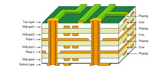
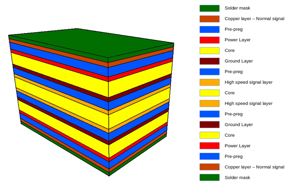
A multilayer PCB is a printed circuit board that comprises three or more conductive layers separated by insulating layers. Unlike single or double-layer PCBs, which feature one or two conductive layers, multilayer PCBs stack multiple layers to accommodate more complex circuitry within a compact space. This structure allows for higher component density, improved signal integrity, and enhanced performance in electronic devices.
2. What Are the Advantages of Using Multilayer PCBs?
Multilayer PCBs offer several significant advantages:
- Enhanced Performance: Multiple layers facilitate better signal routing and reduce electromagnetic interference (EMI), leading to improved overall performance.
- Space-Saving Design: By stacking layers, multilayer PCBs enable more functionality within smaller footprints, making them ideal for compact devices.
- Improved Signal Integrity: Separating power and ground planes minimizes noise and ensures stable power distribution, thereby enhancing signal quality.
3. How Are Multilayer PCBs Manufactured?
Manufacturing multilayer PCBs involves several key steps:
- Design and Layout: Engineers use specialized PCB design software to create the layout, defining the arrangement of layers and component placement.
- Layer Preparation: Each conductive layer is etched onto a substrate material, typically fiberglass-based, to form the circuit patterns.
- Layer Alignment and Lamination: The prepared layers are meticulously aligned and laminated under high pressure and temperature to form a single, cohesive board.
- Drilling and Plating: Precise holes are drilled for vias (vertical interconnections), and these holes are plated with conductive material to establish electrical connections between layers.
- Outer Layer Finishing: The outer surfaces receive protective coatings and solder masks to prevent oxidation and facilitate component soldering.
- Testing and Quality Control: Finished PCBs undergo rigorous testing to ensure they meet specified standards and are free from defects.
4. What Materials Are Used in Multilayer PCBs?
Multilayer PCBs are typically constructed using the following materials:
- Substrate: The base material is usually a fiberglass-reinforced epoxy resin (FR-4), known for its durability and excellent electrical insulation properties.
- Conductive Layers: Copper serves as the standard conductive material due to its superior electrical conductivity. In some high-frequency applications, materials like silver or gold may be used.
- Insulating Layers: High-quality dielectric materials separate the conductive layers, providing electrical isolation while maintaining structural integrity.
5. How Do You Design a Multilayer PCB?
Designing a multilayer PCB involves several critical considerations:
- Layer Stack-Up: Determining the number of layers and their arrangement is crucial for optimizing signal flow and minimizing interference.
- Trace Routing: Efficient routing of electrical traces ensures minimal signal loss and reduces the risk of crosstalk between signals.
- Thermal Management: Incorporating thermal vias and heat sinks helps dissipate heat generated by components, enhancing reliability.
- Software Tools: Advanced PCB design software, such as Altium Designer or Eagle, assists engineers in creating precise and efficient layouts.
Following best practices, such as adhering to design rules, maintaining clearances, and considering manufacturability, ensures the final product meets all performance and quality standards.
6. What Are the Common Applications of Multilayer PCBs?
Multilayer PCBs are versatile and find applications across various industries:
- Consumer Electronics: Smartphones, tablets, laptops, and gaming consoles rely on multilayer PCBs for their compact and high-performance designs.
- Automotive: Advanced driver-assistance systems (ADAS), infotainment systems, and engine control units (ECUs) utilize multilayer PCBs for their reliability and functionality.
- Medical Devices: Equipment like MRI machines, diagnostic instruments, and portable medical devices depend on multilayer PCBs for precision and durability.
- Telecommunications: Routers, switches, and communication infrastructure equipment use multilayer PCBs to handle high-speed data transmission.
- Industrial Automation: Control systems, robotics, and instrumentation devices incorporate multilayer PCBs for their robustness and efficiency.
7. How Do You Ensure Quality in Multilayer PCB Production?
Ensuring quality in multilayer PCB production involves several key measures:
- Material Inspection: We verify the quality of raw materials to meet specified standards.
- Process Control: Monitoring each manufacturing step helps maintain consistency and prevent defects.
- Automated Testing: Utilizing automated optical inspection (AOI) and electrical testing allows us to detect and rectify issues early in the production process.
- Compliance with Standards: Adhering to international standards such as IPC-6011 and ISO 9001 ensures that our PCBs meet industry benchmarks for quality and safety.
- Continuous Improvement: Implementing feedback loops and regular audits helps us identify areas for enhancement and maintain high-quality outputs.
8. What Are the Cost Factors Associated with Multilayer PCBs?
Several factors influence the cost of multilayer PCBs:
- Number of Layers: More layers typically increase production complexity and cost.
- Board Size and Complexity: Larger boards with intricate designs require more materials and precise manufacturing processes.
- Material Selection: High-performance substrates and specialty materials can raise the overall cost.
- Production Volume: Higher volumes often benefit from economies of scale, reducing the per-unit cost.
- Additional Features: Incorporating features like impedance control, high-frequency materials, or embedded components can add to the cost.
- Lead Time: Expedited production schedules may incur additional fees.
Understanding these factors allows for better budgeting and cost management in PCB projects.
9. How Do Multilayer PCBs Compare to Other PCB Types?
Multilayer PCBs offer distinct advantages over single or double-layer PCBs, including:
- Higher Density: They accommodate more components and complex circuitry within a smaller area.
- Improved Performance: Enhanced signal integrity and reduced EMI make them suitable for high-speed and high-frequency applications.
- Better Power Distribution: Dedicated power and ground planes ensure stable power delivery and minimize noise.
However, multilayer PCBs generally cost more and are more complex to manufacture compared to their simpler counterparts. The choice between PCB types depends on the specific requirements of the application, balancing performance needs with budget constraints.
10. What Trends Are Shaping the Future of Multilayer PCBs?
The multilayer PCB industry is evolving with several key trends:
- Miniaturization: As devices become smaller, the demand for more compact and efficient multilayer PCBs increases.
- High-Speed Designs: The rise of 5G, IoT, and advanced computing requires PCBs that can handle higher data rates with minimal signal loss.
- Flexible and Rigid-Flex PCBs: Combining flexibility with multilayer structures opens new possibilities for innovative device designs.
- Advanced Materials: Development of new substrates and conductive materials enhances performance and thermal management capabilities.
- Sustainability: Eco-friendly manufacturing processes and recyclable materials are becoming increasingly important in PCB production.
- Automation and AI: Incorporating automation and artificial intelligence in design and manufacturing processes improves precision and reduces production times.
Staying abreast of these trends ensures that manufacturers and designers can meet the evolving demands of the electronics industry.
Conclusion
Multilayer PCBs are the backbone of modern electronic devices, offering unparalleled performance, compactness, and reliability. Understanding their intricacies—from design and manufacturing to applications and future trends—is essential for engineers and businesses aiming to leverage their full potential. At TriWin Circuits, we specialize in delivering high-quality multilayer PCBs tailored to your specific needs. Whether you’re developing cutting-edge consumer electronics or sophisticated industrial systems, our expertise ensures your projects succeed with precision and excellence. Feel free to reach out to us for more information or to discuss your next PCB project.


