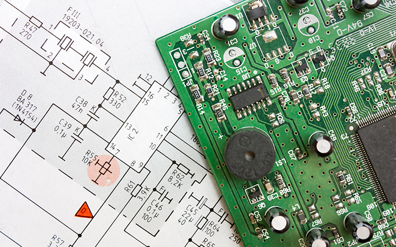
Introduction: Navigating the Cost Landscape
Printed Circuit Boards (PCBs) are the backbone of modern electronic devices. For design engineers and product managers, understanding the factors influencing PCB manufacturing and assembly costs is critical for optimized designs and competitive advantage. This article explores the multifaceted elements that dictate PCB pricing, from design choices and material specifications to manufacturing processes and assembly requirements.
1. Key Cost Drivers in PCB Manufacturing
PCB manufacturing costs are primarily driven by design complexity, specified materials, and production efficiency.
1.1. Design Complexity: The Blueprint of Cost
The inherent complexity of a PCB design significantly influences its manufacturing cost, demanding advanced equipment and intricate processes.
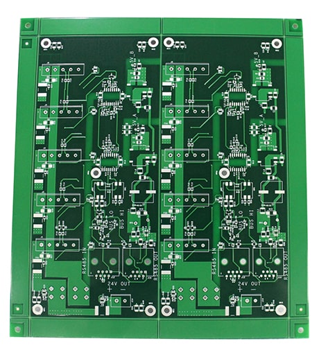
- Layer Count and Stack-up More layers directly increase PCB cost due to additional materials, lamination cycles, and precise alignment requirements. For instance, a four-layer board can be approximately 40% more expensive than a two-layer board.
- Trace Width, Spacing, and Annular Rings Tighter trace widths, spacing, and smaller annular rings (copper pad around a via) demand more advanced imaging, plating, and equipment, increasing costs and potentially affecting yield.
- Drill Holes: Size, Quantity, and Technology The number, size, and variety of drill holes are major cost contributors. Smaller holes (e.g., less than 0.012 inches or 0.2mm) often require expensive laser drilling instead of mechanical drilling, significantly raising costs.
- Special Features: HDI, Rigid-Flex, and Advanced Via Technologies Advanced designs like High-Density Interconnect (HDI) PCBs, Rigid-flex PCBs, or specialized via structures require specific, costly production procedures and tools.
- Vias (Vertical Interconnect Access) are copper-lined holes connecting PCB layers. Their type significantly impacts cost:
- Through-Hole Via (PTH): Extends through the entire board. Cheapest and easiest to manufacture, but consume more space and can cause signal reflection in high-speed designs.
- Blind Via: Connects an outer layer to inner layers, visible on one side. Good for HDI, saving space and improving signal integrity, but more complex and costly (often laser drilled).
- Buried Via: Connects internal layers only, hidden from outer surfaces. Ideal for dense designs and EMI control, but most expensive due to multiple lamination steps.
- Microvia: Very small (under 150 micrometers), laser-drilled, connecting adjacent layers. Crucial for HDI, optimizing space and enhancing signal integrity, but costly.
- Via-in-Pad: Placed directly under a component pad. Shortens trace lengths, beneficial for high-frequency signals, but requires filling and capping, adding complexity and cost.
- Stacked & Staggered Vias: Stacked vias are vertically aligned; staggered are offset. Both are space-efficient, but stacked vias are more costly due to precision fabrication.
- Thermal Vias: Transfer heat from hot components for better dissipation.
- Tented & Filled Vias: Tented vias are solder mask covered for protection; filled vias are filled with epoxy or conductive paste for strength or heat flow. Filling adds 10%+ to cost.
- Design Considerations (affecting cost): Aspect ratio (via depth to diameter) and stub minimization (e.g., back-drilling) impact plating quality, signal integrity, and add significant cost.
Table 1: Overview of PCB Via Types and Their Cost/Performance Trade-offs
| Via Type | Description | Key Advantages | Key Disadvantages | Relative Cost |
| Through-Hole Via (PTH) | Connects all layers, drilled through entire board. | Easy to manufacture, good heat dissipation, structural support. | Consumes space on all layers, potential signal reflection in high-speed designs. | Low |
| Blind Via | Connects outer layer to inner layer, visible on one side. | Space-saving, complex routing, reduced signal loss (shorter path), good for HDI. | More complex and costly than PTH, requires precise drilling (often laser). | Medium |
| Buried Via | Connects only internal layers, hidden from outer surfaces. | Ideal for dense multilayer designs, space efficiency, EMI control. | Most expensive to manufacture, requires multiple lamination steps. | High |
| Microvia | Very small (under 150 µm), laser-drilled, connects adjacent layers. | Optimizes routing space, enhances signal integrity (reduced parasitics), enables denser designs. | Intricate and costly production process, requires specialized laser drilling. | High |
| Via-in-Pad | Placed directly under component pad (e.g., BGA). | Shortens trace lengths, beneficial for high-frequency signals, reduces solder bridging. | Requires filling and capping to prevent solder flow, adds manufacturing complexity. | Medium-High |
| Stacked Vias | Vias aligned vertically across multiple layers. | Space-efficient for multi-layer connections. | High manufacturing costs due to precision drilling and electroplating. | High |
| Staggered Vias | Vias offset across different layers. | Optimizes routing, reduces signal interference, efficient use of space. | More complex to design than stacked vias. | Medium-High |
| Thermal Vias | Designed to transfer heat from hot components. | Enhances heat dissipation, improves board reliability. | Adds to drill count and complexity, requires strategic placement. | Low-Medium |
| Tented Vias | Covered with solder mask. | Protects copper ring from moisture/damage, reduces shorts. | May trap air/flux if not properly executed. | Low |
| Filled Vias | Filled with epoxy (non-conductive) or conductive paste. | Strengthens via, improves heat flow (conductive fill), provides flat surface for component placement. | Adds 10%+ to cost, specialized filling/capping processes. | Medium-High |
1.2. Material Selection: Foundation of Expense
Raw material choice directly impacts PCB cost and performance.
- Substrate Type and Thickness Standard FR-4 is economical, but high-frequency materials (e.g., Rogers), metal-core PCBs, or flexible materials are more expensive due to specialized properties and processing. Thicker boards also cost more.
- Copper Weight and Thickness Thicker copper layers (e.g., 2 oz. or more) increase cost due to higher material usage and complex processing like longer etching times.
- Surface Finish and Solder Mask Surface finishes like Organic Solder Preservative (OSP) and Hot Air Solder Leveling (HASL) are lowest cost. Advanced finishes like Electroless Nickel Immersion Gold (ENIG) are more expensive due to materials and complex processes.
Table 2: Comparison of Common PCB Surface Finishes and Cost Implications
| Finish Type | Key Characteristics | Relative Cost | Common Applications |
| OSP (Organic Solder Preservative) | Excellent flatness, good for fine pitch, limited shelf life, not ideal for multiple reflows. | Lowest | Consumer electronics, high-volume, cost-sensitive products. |
| HASL (Hot Air Solder Leveling) – Leaded | Good solderability, low cost, uneven surface, not RoHS compliant. | Low | General purpose, less critical applications. |
| HASL (Hot Air Solder Leveling) – Lead-Free | Good solderability, cost-effective, uneven surface, RoHS compliant. | Low | General purpose, RoHS compliant products. |
| Immersion Tin (ImSn) | Excellent flatness, good for fine pitch, good solderability, short shelf life, tin whiskers concern. | Medium | Fine pitch, flat surface requirements, short-term storage. |
| Immersion Silver (ImAg) | Very good flatness, good for fine pitch, good solderability, sensitive to handling/storage. | Medium | Fine pitch, high-frequency, complex designs. |
| ENIG (Electroless Nickel Immersion Gold) | Excellent flatness, long shelf life, good for fine pitch, good for wire bonding. | High | HDI, BGA, fine pitch, high reliability, wire bonding. |
| Flash Gold | Thin gold layer over nickel, good wire bonding, moderate solderability. | High | Keypads, switch contacts, edge connectors. |
| Hard Gold Plating | Thick, durable gold layer over nickel, excellent wear resistance, poor solderability. | Highest | Edge connectors, switch contacts, high-wear applications. |
1.3. Production Efficiency & Logistics
Manufacturing efficiency and logistics significantly impact final PCB cost.
- Panel Utilization and Board Size/Shape Larger or irregularly shaped PCBs use more raw materials and can increase production difficulty. Efficient panel utilization (above 80% is good) reduces waste and costs.
- Manufacturing Tolerances and IPC Class Stricter manufacturing tolerances and higher IPC (Association Connecting Electronics Industries) classes (e.g., Class 3 for high-reliability) demand tighter process controls, rigorous inspection, and higher-grade materials, all increasing costs.
- Lead Time and Turnaround Speed Short lead times significantly increase costs due to expedited processes, overtime, and re-prioritization. Rush orders can add a premium of 30% to 200% and require expensive logistics.
2. Key Cost Drivers in PCB Assembly
PCB assembly costs are influenced by component characteristics, assembly methods, and quality assurance.
2.1. Component-Related Factors
Component type, quantity, and packaging are primary determinants of assembly cost.
- Component Type, Quantity, and Sourcing High-end, specialized, or hard-to-find components increase material cost and lead times. The sheer number of components also affects assembly time and complexity.
- Component Packaging (SMT vs. Through-Hole, Fine-Pitch, BGAs) Surface Mount Technology (SMT) assembly is generally less expensive and faster due to automation. Through-Hole Technology (THT) often requires manual insertion, adding costs. Fine-pitch parts or Ball Grid Arrays (BGAs) demand precise machinery and X-ray inspection, significantly increasing costs.
2.2. Assembly Process and Quality
Assembly efficiency, labor, and quality control directly impact the final price.
- Labor Costs and Geographic Location Labor costs vary significantly by region. Lower labor cost countries can offer savings, but these may be offset by increased shipping, communication delays, and potential quality issues.
- Testing and Quality Control Rigorous testing (e.g., Automated Optical Inspection (AOI), X-ray inspection, functional testing) ensures reliability but adds to the cost, potentially 10% to 15% for inspection alone.
- Special Assembly Processes Additional services like conformal coating, underfill, selective soldering, or custom labeling add extra steps, materials, and labor, increasing assembly costs.
2.3. Overhead and Logistics
Overhead and logistics contribute significantly to the final price.
- Equipment, Tooling, and Facility Overhead Fixed costs like machine depreciation, maintenance, and facility expenses are distributed across assembled units. For small batches, these setup costs form a larger proportion of the per-unit price.
- Packaging and Shipping Packaging and shipping costs, especially for overseas manufacturing or rush orders, can add up quickly and erode savings from lower labor costs.
3. Strategies for Cost Optimization and Value Engineering
Understanding cost drivers is the first step; actively implementing strategies to optimize them is where true value engineering lies.
3.1. Design for Manufacturability (DFM) and Assembly (DFA)
Early collaboration with manufacturers and proactive DFM/DFA checks identify and address potential issues early, saving time and avoiding costly errors or rework.
Optimization through DFM/DFA includes:
- Simplify Design: Minimize layers, avoid complex geometries, use standard trace widths/spacing.
- Standardize Vias: Prioritize through-hole vias; use advanced vias only when essential. Optimize via sizes and aspect ratios.
- Component Selection: Favor readily available, standard components (SMT over THT where feasible). Design for automated assembly.
- Tolerance Relaxation: Relax tolerances and IPC class if not critical for the application.
3.2. Strategic Material and Component Sourcing
Strategic sourcing involves finding the best value, understanding market trends, negotiating terms, and building long-term partnerships for stable pricing and supply chain resilience.
Key actions include:
- Balance Performance and Cost: Choose materials that meet requirements without over-specifying.
- Leverage Supplier Relationships: Collaborate with manufacturers and suppliers for cost-effective alternatives or bulk pricing.
- Multi-Sourcing: Identify multiple reputable suppliers for critical components to mitigate risks.
3.3. Volume, Lead Time, and Supplier Collaboration
Production volume, lead time, and effective communication significantly impact cost. Strong supplier relationships lead to better pricing and support.
Key actions include:
- Optimize Production Volume: Leverage economies of scale by ordering larger quantities.
- Plan Lead Times: Avoid rush orders by planning in advance; longer lead times allow better pricing.
- Foster Communication: Maintain clear communication with your PCB supplier to avoid delays and added costs.
Table 3: Key Strategies for PCB Cost Reduction
| Strategy Area | Specific Action | Expected Cost Impact |
| Design | Optimize Layer Count (use fewest necessary) | Significant Savings |
| Simplify Board Geometry (rectangular, standard sizes) | Moderate Savings | |
| Relax Trace Width/Spacing Tolerances (if applicable) | Moderate Savings | |
| Standardize Via Types (prioritize PTH) | Moderate Savings | |
| Optimize Via Sizes and Aspect Ratios | Moderate Savings | |
| Materials | Use Standard Substrate Materials (e.g., FR-4) | Significant Savings |
| Select Copper Weight Based on Actual Needs | Moderate Savings | |
| Choose Cost-Effective Surface Finishes (e.g., OSP, HASL) | Moderate Savings | |
| Process | Plan for Longer Lead Times (avoid rush orders) | Avoids High Premiums |
| Optimize Production Volume (leverage economies of scale) | Significant Savings | |
| Select Appropriate IPC Class (avoid over-specification) | Moderate Savings | |
| Supply Chain | Multi-Source Critical Components | Avoids Premiums, Enhances Stability |
| Foster Strong Supplier Relationships | Long-term Savings, Improved Support | |
| Implement DFM/DFA Early in Design Cycle | Significant Savings (prevents costly errors) |
Conclusion: Mastering PCB Costs for Competitive Advantage
PCB manufacturing and assembly costs are influenced by a complex interplay of design choices, material science, manufacturing processes, and supply chain dynamics. By understanding these factors, electronics professionals can move beyond reactive cost management to proactive value engineering. Balancing performance with cost-effective design and production strategies is crucial for innovation, faster time-to-market, and competitive advantage. Continuous collaboration between design, engineering, procurement, and manufacturing teams, coupled with a commitment to DFM/DFA principles, will be key to future cost optimization in PCB production.
At Triwin, we excel at navigating these complex cost drivers to deliver high-reliability PCBs and comprehensive assembly solutions. Our expertise in advanced PCB manufacturing, including diverse via technologies and material options, combined with rigorous quality control and a customer-centric approach, ensures optimal performance and cost-efficiency for your projects. We are committed to being your “All-Around PCB Supplies Solution,” helping you achieve competitive pricing without compromising on quality or reliability.


