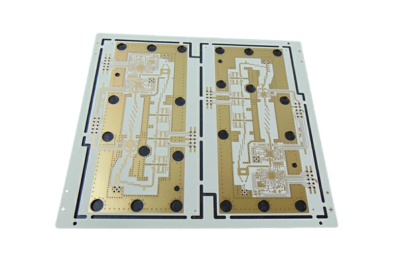
High-Speed PCB Manufacturing Service
At TriWin, we specialize in High-Speed PCBs, the core components for today’s most advanced digital systems. As data rates soar, ensuring signal integrity is critical. Our expertise guarantees your designs achieve peak performance, enabling faster, more reliable data transmission in complex applications. Discover how TriWin’s precision manufacturing capabilities and deep understanding of High-Speed PCB principles provide the reliable foundation your innovations need.
Defining High-Speed Signals and High-Speed Design
A High-Speed PCB is designed to handle digital signals with extremely fast rise and fall times. While clock frequency is often cited, it’s the signal’s rise/fall time, not just its frequency, that primarily determines if a design requires “high-speed” considerations. If a signal’s transition time is faster than twice the propagation delay of the trace, it behaves as a transmission line, and high-speed design rules become critical.
This introduces the concept of “critical length.” When a trace length exceeds a specific proportion of the signal’s wavelength (typically 1/10th or 1/7th), it acts as a transmission line, requiring precise impedance control to avoid reflections.
At its core, high-speed design is about preserving Signal Integrity (SI). This means ensuring that digital signals arrive at their destination accurately, without distortion, reflections, or excessive delay.

PCB manufacturing

High-Speed PCB vs. High-Frequency PCB
While often confused due to overlapping challenges, High-Speed PCBs and High-Frequency PCBs have distinct primary focuses:
- High-Speed PCB Design: Primarily concerns fast-edge digital signals and their integrity. The focus is on preventing issues like reflections, crosstalk, timing errors, and power integrity problems that arise from rapid voltage transitions. These boards are common in computing, data centers, and digital communication interfaces.
- High-Frequency PCB Design: Primarily concerns analog RF/Microwave signals and their transmission loss. The focus is on minimizing signal attenuation (due to dielectric loss), maintaining stable impedance, and ensuring consistent dielectric constant (Dk) and dissipation factor (Df) for high-power or sensitive RF applications. These boards are prevalent in wireless communications, radar, and satellite systems.
Although they both demand specialized materials and precise manufacturing, their fundamental challenges and optimization priorities differ.
Why is Signal Integrity Crucial?
In High-Speed PCB designs, even minor signal degradation can lead to system malfunction, data errors, or complete failure. Maintaining Signal Integrity (SI) is paramount to ensure the reliable operation of digital circuits.
Key Issues Affecting Signal Integrity:
- Reflections: Caused by impedance mismatches along a trace, leading to portions of the signal bouncing back and interfering with the original signal. This can result in false triggering or missed bits.
- Ringing & Overshoot: When signals oscillate rapidly above or below their stable logic levels before settling, potentially causing component damage or false switching.
- Crosstalk: Unwanted electromagnetic coupling between adjacent signal traces, where a signal on one trace induces noise on another. This can corrupt data.
- Timing Issues & Signal Skew: Variations in signal propagation delays across different traces within a bus, leading to signals arriving at different times and causing data errors or reducing clock speeds.
- Ground Bounce: Fluctuations in the ground reference voltage caused by large, fast current changes from switching digital components, which can affect voltage levels across the board.

Core Principles & Best Practices for High-Speed PCB Design
Achieving robust Signal Integrity in High-Speed PCBs requires adherence to specific design principles and best practices.
Strategic PCB Stack-up Design
Optimizing the PCB stack-up is foundational for managing signal integrity.
- Multi-Layer Board Design: Strategic placement of signal layers, dedicated ground planes, and power planes is crucial. Ground and power planes provide stable reference voltages and return paths, minimizing noise.
- Continuous, Uninterrupted Ground Planes: Solid ground planes are essential for providing low-impedance return paths for high-speed signals, mitigating EMI and crosstalk. Avoid splitting ground planes under high-speed traces.
Via Design and Optimization
Vias are necessary but introduce parasitic capacitance and inductance that can degrade signal quality.
- Parasitic Effects: Each via adds parasitic capacitance and inductance, which can create impedance discontinuities at high speeds.
- Back Drilling: This crucial technique involves drilling out the unused portion of a via barrel (the "stub") that extends beyond the connected layers. Back drilling significantly reduces reflections caused by these stubs in high-speed transmission lines.
- Ground Stitching Vias: Strategically placing vias to connect ground planes on different layers helps to create a low-impedance return path for signals and improve overall grounding effectiveness.
High-Speed Routing Strategies
Precise routing strategies are critical for managing signal propagation and minimizing integrity issues.
- Trace Length & Matching: For critical networks (e.g., DDR buses, PCIe), trace lengths must be precisely matched to ensure all bits arrive simultaneously, preventing timing issues and signal skew.
- Differential Pair Routing: Differential pairs must be routed with equal lengths, kept in close proximity (tightly coupled), and maintain consistent spacing to maximize common-mode noise rejection and minimize EMI.
- Avoiding 90-Degree Bends: Sharp 90-degree turns can cause impedance discontinuities and reflections. Using 45-degree angles or smooth arcs is preferred.
The 3W & 20H Rules:
3W Rule: Maintain a minimum spacing of 3 times the trace width between adjacent signal traces to reduce crosstalk.
20H Rule: Keep critical power and ground planes within 20 times the dielectric height from the edge of the board to contain electromagnetic fields and reduce EMI.
Controlled Impedance
Controlled impedance is vital to prevent reflections in high-speed circuits.
- Characteristic Impedance & Differential Impedance: Understanding these concepts is key. Characteristic impedance (typically 50 Ohms for single-ended, 100 Ohms for differential) must be maintained along the signal path.
- Precise Control: Impedance is precisely controlled by the trace width, copper thickness, dielectric constant (Dk) of the material, and the thickness of the dielectric layer.
- Taconic: Provides PTFE and woven fiberglass/ceramic filled laminates with stable electrical properties.
Microstrip and Stripline:
Microstrip: A trace on an outer layer with a ground plane directly below it. Simpler to manufacture but more susceptible to external noise and EMI radiation.
Stripline: A trace embedded between two ground planes. Offers better EMI shielding and signal integrity but requires more layers.
Component Placement Strategy:
Thoughtful component placement minimizes trace lengths and optimizes signal flow.
- Modular Layout: Group related components and functional blocks (e.g., power supply, CPU, memory interface) to minimize signal path lengths.
- Proximity to Interference Sources: Place high-speed components away from noise-sensitive circuits and interference sources.
- Shortening Critical Paths: Position components to minimize the length of crucial signal paths, reducing delay and signal degradation.
- Decoupling Capacitor Placement: Place decoupling capacitors as close as possible to the power pins of ICs (especially high-speed ones) to provide localized, low-impedance power delivery and absorb transient current demands.
High-Frequency PCB Design and Manufacturing Considerations
Successful High-Frequency PCB performance hinges on stringent design practices and highly specialized manufacturing capabilities.
Critical Design Guidelines for Signal Integrity
Designing for High-Frequency PCBs goes beyond basic connectivity to ensure signal integrity and minimal loss:
- Impedance Control: Crucial for high-frequency signals, maintaining consistent characteristic impedance throughout the trace (e.g., 50 Ohm or 75 Ohm) is paramount to prevent signal reflections. This requires precise control over trace width, copper thickness, and dielectric constant/thickness.
- Trace Width and Spacing: Accurate trace geometry directly affects impedance and signal loss. Controlled impedance routing uses precise trace widths and spacing to achieve the target impedance. Wider spacing can minimize crosstalk.
- Minimizing Crosstalk: Techniques like sufficient spacing between signal traces, using guard traces, and proper grounding are employed to reduce unwanted electromagnetic coupling between adjacent signals.
- Via Design: Vias, while necessary, introduce parasitic capacitance and inductance. Proper via placement, minimizing via stub lengths (back drilling), and utilizing microvias can significantly reduce these parasitic effects in high-frequency paths.
- Grounding Techniques: A solid, continuous ground plane is essential for providing a stable reference voltage and minimizing noise. Multiple ground vias should be used to stitch ground planes together, especially in multi-layer designs.
- Routing Optimization: Using shorter trace lengths, avoiding sharp bends (preferring gentle curves), and careful differential pair routing are critical to maintaining signal integrity and minimizing reflections at high frequencies.

Our Advanced Manufacturing Capabilities
TriWin combines unparalleled expertise with state-of-the-art technology to manufacture High-Frequency PCBs that meet the most stringent performance requirements.
Specialized Material Handling
Our facilities are equipped to precisely handle and process delicate and specialized high-frequency laminates, including PTFE-based materials, requiring specific lamination and drilling techniques.
Precision Photolithography & Etching
We utilize advanced imaging and etching processes to achieve the extremely fine lines and spaces required for accurate impedance control and high-density routing.
Advanced Drilling Technology
Employing laser drilling for microvias and specialized mechanical drilling for challenging HF materials ensures precise hole formation with minimal damage to the laminate. Back drilling capabilities are available to remove unwanted via stubs, critical for signal integrity.
Rigorous Plating Processes
Our plating lines are optimized to ensure uniform copper deposition within holes and on traces, crucial for consistent impedance and reliable interconnections.
Automated Optical Inspection (AOI)
High-resolution AOI systems are used to inspect every layer for defects, ensuring pattern accuracy.
Electrical Testing (E-Test) & Impedance Testing
Every board undergoes 100% electrical testing. Crucially, we perform Impedance Control Testing using advanced Time Domain Reflectometry (TDR) to verify characteristic impedance on critical traces.
Controlled Lamination
Our lamination processes are precisely controlled for temperature, pressure, and vacuum, ensuring optimal bond strength and preventing delamination of complex HF material stacks.
Our High-Speed PCB Manufacturing Capabilities
At TriWin, our commitment to excellence is reflected in our advanced High-Speed PCB manufacturing capabilities, ensuring your designs are brought to life with precision and reliability.
Extensive Experience
With years of dedicated experience in the demanding field of High-Speed PCB manufacturing, we have a proven track record of successfully delivering complex projects for leading technology companies.
State-of-the-Art Equipment
Our facilities are equipped with the latest advanced manufacturing technology. This includes highly precise photolithography for fine lines, advanced etching capabilities, specialized drilling machines (including laser drilling), and controlled lamination presses, all designed to meet the tight tolerances of high-speed designs.
Rigorous Quality Control
Quality is paramount for high-speed performance. We implement stringent quality assurance protocols at every stage, including.
Professional Engineering Support
Our team of highly skilled engineers specializes in High-Speed PCB design for manufacturability (DFM). We collaborate closely with your design team to identify potential issues early, optimize stack-ups, recommend materials, and ensure your design achieves optimal performance and yields.
