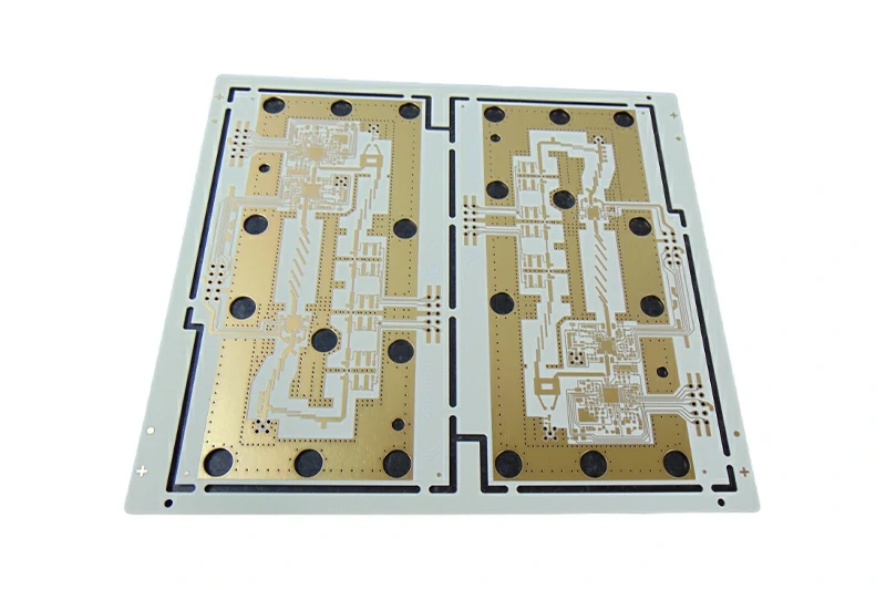
High Frequency PCB Manufacturing Service
At TriWin Circuits, we specialize in High-Frequency PCBs. These boards provide the essential technology for next-gen electronics, ensuring optimal signal integrity and performance in your most demanding applications. With our expertise in High-Frequency PCB design, materials, and manufacturing, we empower innovations in areas like 5G infrastructure and automotive radar with faster, more reliable signal transmission.
What is a High-Frequency PCB?
High-Frequency PCBs are specialized Printed Circuit Boards designed to handle electronic signals that operate at high speeds, typically ranging from 500MHz to 2GHz and well beyond. In these frequency ranges, the behavior of signals on a PCB differs significantly from lower frequencies, requiring unique materials and design principles to prevent signal degradation.
It’s important to distinguish between related terms:
- High-Frequency PCBs: A broad category for boards operating at high electromagnetic frequencies.
- High-Speed PCBs: Often refers to digital signals with fast rise/fall times, where signal integrity issues (like reflections and crosstalk) become critical, even if the fundamental clock frequency isn't extremely high.
- RF (Radio Frequency) PCBs: Specifically designed for radio frequency applications, typically from a few MHz up to a few GHz.
- Microwave PCBs: Designed for even higher frequencies, generally from 1 GHz up to 300 GHz.
All these categories share the common characteristic of demanding precise control over electrical properties to ensure faster signal flow and reliable operation within their specified higher frequency ranges.

PCB manufacturing

Why are High-Frequency PCBs Essential?
The rapid evolution of technology has led to an increasing demand for faster data transmission and higher bandwidth in almost every modern electronic device. Standard FR-4 PCBs, while suitable for many applications, introduce unacceptable levels of signal loss and distortion at high frequencies.
High-Frequency PCBs are essential because they directly impact signal integrity and overall performance. They provide a stable and controlled environment for high-speed signals, minimizing issues like attenuation, reflections, and crosstalk. This role is critical in enabling cutting-edge technologies, including:
- 5G and future wireless communication infrastructure
- IoT (Internet of Things) devices with advanced connectivity
- Advanced Driver-Assistance Systems (ADAS) in automotive applications
- High-speed data networks, satellite communication, and radar systems.
Key Characteristics and Properties of High-Frequency PCBs
The performance of High-Frequency PCBs is fundamentally determined by the properties of their specialized dielectric materials.
Low and Stable Dielectric Constant (Dk)
- Explanation: The Dielectric Constant (Dk), or relative permittivity, measures a material's ability to store electrical energy. In High-Frequency PCBs, Dk directly influences the speed at which an electrical signal propagates through the material.
- Importance: A lower Dk value minimizes signal delay and ensures faster signal transmission. Crucially, the Dk must remain stable across varying frequencies and temperatures to guarantee consistent impedance and predictable circuit behavior.
Low Dissipation Factor (Df)
- Explanation: The Dissipation Factor (Df), also known as tangent loss (tan δ), quantifies the rate at which electrical energy is absorbed by the dielectric material and converted into heat.
- Importance: A lower Df value is critical for minimizing signal attenuation (loss of signal strength) and ensuring better signal quality. Low Df directly contributes to reduced power consumption and improved signal transmission efficiency, especially vital in RF and microwave circuits.
Low Coefficient of Thermal Expansion (CTE)
- Importance: The Coefficient of Thermal Expansion (CTE) describes how much a material expands or contracts with changes in temperature. For High-Frequency PCBs, a low CTE is crucial for thermal stability and reliability, particularly in applications experiencing significant temperature fluctuations.
- Impact: A CTE that closely matches that of the copper foil and attached components (like ICs) prevents stress on solder joints and plated through-holes, significantly reducing the risk of delamination, cracks, and improving long-term reliability.
Other Important Properties
Beyond Dk, Df, and CTE, other properties are vital for High-Frequency PCB performance:
- Low Moisture Absorption: Moisture can significantly increase Dk and Df, degrading signal integrity. Materials with low moisture absorption maintain stable electrical properties.
- Excellent Thermal Resistance: The ability of the material to withstand high operating temperatures without degradation of its electrical or mechanical properties.
- Chemical Resistance and Peel Strength: Ensures the PCB can withstand manufacturing processes and harsh operating environments, maintaining the bond between copper and the dielectric.
High-Frequency PCB Materials: The Foundation of Performance
Choosing the Right Material for Your Application
The material selection is arguably the most critical factor in High-Frequency PCB performance. It directly dictates the board’s electrical properties, thermal stability, and manufacturability. Engineers must carefully consider:
- Frequency of operation: Higher frequencies demand lower Dk and Df.
- Signal speed and integrity requirements: Dictates impedance control needs.
- Thermal conditions: Operating temperature range and heat dissipation needs.
- Cost considerations: Balancing performance with budget.

Common High-Frequency PCB Materials
TriWin Circuits works with a wide range of specialized high-frequency PCB materials to meet diverse application requirements
Rogers Materials: Leading the industry, Rogers offers a variety of high-performance laminates.
- RO4000 series (e.g., RO4350B, RO4003C): Excellent electrical properties (low Dk/Df), good thermal management, and often more cost-effective than PTFE, suitable for high-volume RF applications.
- RO3000 series (e.g., RO3003, RO3006): Ceramic-filled PTFE composites with very stable Dk/Df over temperature, ideal for sensitive high-frequency circuits.
- RT/Duroid series: PTFE/woven fiberglass laminates, known for extremely low Dk/Df and excellent stability, preferred for the most demanding microwave and millimeter-wave applications.
Teflon (PTFE):
- Properties: Polytetrafluoroethylene (PTFE)-based laminates offer exceptional electrical properties, extremely low Dk and Df, and high thermal resistance.
- Applications: Ideal for very high-frequency (mmWave) applications, high-power RF, and demanding environments.
FR-4 (High-Performance):
- Properties: While standard FR-4 is not suitable for high frequencies, certain high-performance FR-4 variants with improved Dk, Df, and stability can be used. These often feature specialized resin systems.
- Limitations: Still have higher Dk/Df compared to specialized HF laminates.
- Applications: Can be a cost-effective option for some lower-end high-frequency applications (e.g., up to a few GHz) or often used in hybrid constructions (combining HF material layers with FR-4 core layers).
Other Specialized Materials: TriWin also works with laminates from other reputable manufacturers like:
- Panasonic Megtron series: Known for very low Dk/Df and excellent thermal reliability for high-speed digital and RF applications.
- Isola: Offers a range of low-loss materials for high-speed digital and RF.
- Taconic: Provides PTFE and woven fiberglass/ceramic filled laminates with stable electrical properties.
Material Comparison Table
To aid in material selection, here’s a simplified comparison of common high-frequency PCB material types
| Material Type | Typical Dk (10GHz) | Typical Df (10GHz) | Typical CTE (ppm/°C, Z-axis) | Relative Cost | Common Applications | |||
| Rogers RO4350B | 3.48 | 0.0037 | 30 (Z) | Medium-High | 5G Antennas, Automotive Radar, Amplifiers | |||
| Rogers RO3003 | 3 | 0.001 | 24 (Z) | High | GPS Antennas, Satellite Communications, Phase Array Antennas | |||
| PTFE/Teflon-based | 2.2 – 2.6 | < 0.001 | 200+ (Z, uncured) | Very High | Extremely High-Frequency, Microwave, RF/mmWave | |||
| High-Perf FR-4 | 3.8 – 4.5 | 0.008 – 0.015 | 40 – 60 (Z) | Low-Medium | Lower GHz RF, High-Speed Digital (cost-sensitive) | |||
High-Frequency PCB Design and Manufacturing Considerations
Successful High-Frequency PCB performance hinges on stringent design practices and highly specialized manufacturing capabilities.
Critical Design Guidelines for Signal Integrity
Designing for High-Frequency PCBs goes beyond basic connectivity to ensure signal integrity and minimal loss:
- Impedance Control: Crucial for high-frequency signals, maintaining consistent characteristic impedance throughout the trace (e.g., 50 Ohm or 75 Ohm) is paramount to prevent signal reflections. This requires precise control over trace width, copper thickness, and dielectric constant/thickness.
- Trace Width and Spacing: Accurate trace geometry directly affects impedance and signal loss. Controlled impedance routing uses precise trace widths and spacing to achieve the target impedance. Wider spacing can minimize crosstalk.
- Minimizing Crosstalk: Techniques like sufficient spacing between signal traces, using guard traces, and proper grounding are employed to reduce unwanted electromagnetic coupling between adjacent signals.
- Via Design: Vias, while necessary, introduce parasitic capacitance and inductance. Proper via placement, minimizing via stub lengths (back drilling), and utilizing microvias can significantly reduce these parasitic effects in high-frequency paths.
- Grounding Techniques: A solid, continuous ground plane is essential for providing a stable reference voltage and minimizing noise. Multiple ground vias should be used to stitch ground planes together, especially in multi-layer designs.
- Routing Optimization: Using shorter trace lengths, avoiding sharp bends (preferring gentle curves), and careful differential pair routing are critical to maintaining signal integrity and minimizing reflections at high frequencies.

Our Advanced Manufacturing Capabilities
TriWin combines unparalleled expertise with state-of-the-art technology to manufacture High-Frequency PCBs that meet the most stringent performance requirements.
Specialized Material Handling
Our facilities are equipped to precisely handle and process delicate and specialized high-frequency laminates, including PTFE-based materials, requiring specific lamination and drilling techniques.
Precision Photolithography & Etching
We utilize advanced imaging and etching processes to achieve the extremely fine lines and spaces required for accurate impedance control and high-density routing.
Advanced Drilling Technology
Employing laser drilling for microvias and specialized mechanical drilling for challenging HF materials ensures precise hole formation with minimal damage to the laminate. Back drilling capabilities are available to remove unwanted via stubs, critical for signal integrity.
Rigorous Plating Processes
Our plating lines are optimized to ensure uniform copper deposition within holes and on traces, crucial for consistent impedance and reliable interconnections.
Automated Optical Inspection (AOI)
High-resolution AOI systems are used to inspect every layer for defects, ensuring pattern accuracy.
Electrical Testing (E-Test) & Impedance Testing
Every board undergoes 100% electrical testing. Crucially, we perform Impedance Control Testing using advanced Time Domain Reflectometry (TDR) to verify characteristic impedance on critical traces.
Controlled Lamination
Our lamination processes are precisely controlled for temperature, pressure, and vacuum, ensuring optimal bond strength and preventing delamination of complex HF material stacks.
Why Choose Us for Your High-Frequency PCB Needs?
When your application demands uncompromising performance at high frequencies, TriWin Circuits is your trusted partner.
Unmatched Expertise and Experience:
- Deep Industry Knowledge: With years of experience in the PCB industry, TriWin possesses a profound understanding of the complexities inherent in High-Frequency PCB design and manufacturing.
- Skilled Engineering Team: Our dedicated team of skilled engineers specializes in RF, microwave, and high-speed digital PCB layout and fabrication. They provide expert DFM (Design for Manufacturability) support, ensuring your designs are optimized for performance and production efficiency.
State-of-the-Art Technology:
- Advanced Manufacturing Equipment: Our facilities are equipped with state-of-the-art laser drilling machines, precision lamination presses, and highly accurate etching equipment specifically designed to handle delicate high-frequency laminates and achieve tight tolerances.
- Specialized Testing Capabilities: We employ advanced testing equipment, including Time Domain Reflectometry (TDR) for precise impedance control, network analyzers for material characterization, and comprehensive electrical test systems, ensuring every board meets stringent specifications.
Commitment to Quality:
- Rigorous Quality Management System: TriWin operates under a strict quality management system, ensuring consistent quality control at every stage of the manufacturing process, from material inspection to final product testing.
- Industry Certifications: Our adherence to global quality and environmental standards, including ISO 9001, IATF 16949 (Automotive standard), ISO 14001 (Environmental management), and UL certifications, reflects our unwavering commitment to producing reliable, high-performance PCBs.
Excellent Customer Support:
- Responsive and Knowledgeable Team: We pride ourselves on providing responsive and helpful customer service. Our technical support team is ready to assist you with inquiries, design challenges, and project updates, ensuring a smooth and collaborative experience.
- Collaborative Partnership: We work closely with our clients throughout the entire project lifecycle, offering valuable insights and solutions to achieve optimal results for their High-Frequency PCB requirements.
