HDI PCBs: Advanced Solutions for High-Density Interconnects
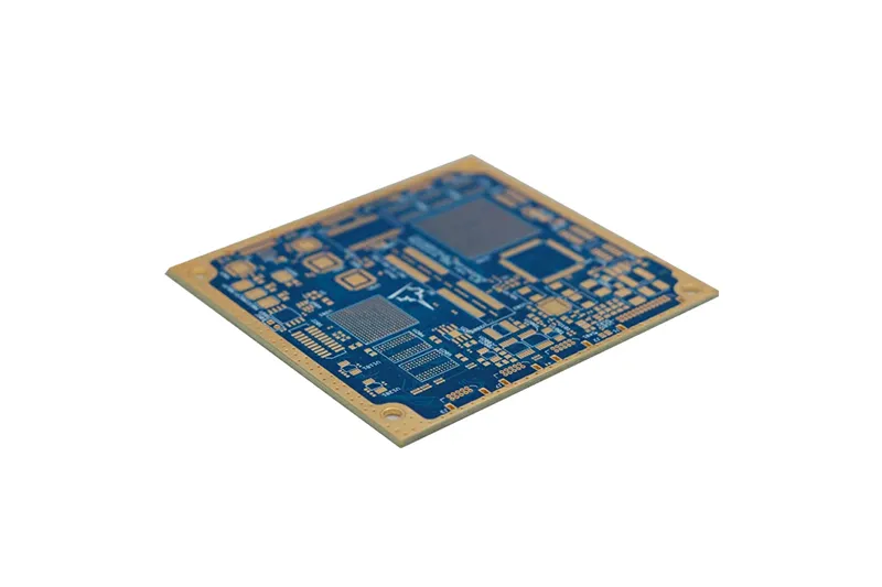
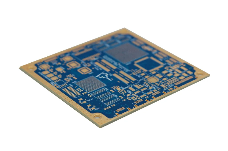
At TriWin Circuits, we specialize in HDI (High-Density Interconnect) PCBs, offering cutting-edge solutions for compact and high-performance electronic designs. Our HDI PCBs are engineered to meet the demands of miniaturization and increased functionality, providing superior signal integrity and reliability for complex applications. TriWin’s expertise in HDI PCB manufacturing helps you achieve higher circuit density, enhanced electrical performance, and smaller product footprints.
What Are HDI PCBs?
HDI PCBs represent a significant advancement in Printed Circuit Board technology. They feature a higher wiring density per unit area than conventional PCBs, primarily achieved through the use of microvias (drilled holes typically less than 0.15mm in diameter), buried vias, and laser drill technology. This construction allows for more components on less board space and improved electrical performance.
Unlike traditional PCBs that use mechanical drilling, HDI PCBs rely on laser drilling for their microvias. These tiny vias connect layers in a more flexible and efficient manner, enabling finer lines and pads. HDI technology is defined by features like:
- Microvias: Small holes (typically 6mil or less) that connect adjacent layers.
- Blind Vias: Vias that connect an outer layer to an inner layer but don't go all the way through the board.
- Buried Vias: Vias that connect two or more inner layers and are not visible from the outer layers.
- Fine Lines and Spacing: Enabling higher circuit density.
- High Layer Count: Allowing for complex routing in a compact design.
PCB manufacturing
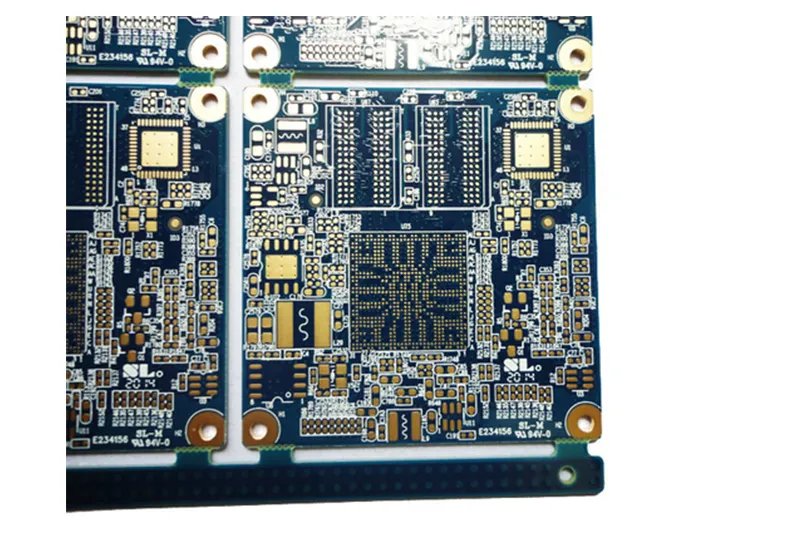
Types of HDI PCB Stack-ups
The design flexibility of HDI PCBs is greatly influenced by their stack-up configuration, which describes how microvias are stacked or staggered across layers. TriWin offers various HDI stack-up types to suit diverse design complexities
1+N+1 HD
This is the simplest HDI structure, featuring one layer of HDI on each side of a conventional core. It uses one set of sequential laminations, incorporating microvias on the outer layers connected to the first inner layers.
2+N+2 HDI
This configuration involves two layers of HDI on each side of the core, requiring two sets of sequential laminations. It allows for higher routing density than 1+N+1, connecting outer layers to deeper inner layers.
Any-Layer HDI (ELIC - Every Layer Interconnect)
This is the most advanced HDI type, where every layer can be interconnected with microvias. This technology offers maximum routing flexibility and density, crucial for highly complex and miniaturized designs. Each layer in an ELIC board can contain microvias that connect to any other layer, enabling extremely compact and efficient designs.
Key Advantages of TriWin HDI PCBs
Choosing TriWin’s HDI PCB solutions offers distinct benefits crucial for modern electronic designs:
Increased Circuit Density: HDI PCBs allow for more components and greater routing complexity in a smaller area. This enables miniaturization and higher functionality in your products.
Enhanced Electrical Performance: The use of microvias and shorter signal paths in HDI PCBs reduces signal integrity issues like crosstalk and impedance mismatches, leading to improved high-frequency performance and better signal quality.
Improved Reliability: The smaller, more precisely drilled microvias are less prone to stress than larger through-holes, which can increase the overall durability and reliability of the board, especially under thermal cycling.
Cost-Effectiveness for Complex Designs: While initial costs might seem higher than conventional PCBs, HDI PCBs can reduce overall system costs by minimizing board size, simplifying assembly, and improving product performance, ultimately leading to higher yields and reduced material waste.
Weight Reduction: The ability to achieve higher functionality in a smaller footprint often results in lighter products, which is critical for portable devices and aerospace applications.
TriWin's HDI PCB Manufacturing Capabilities & Specifications
TriWin Circuits is equipped with advanced capabilities to produce high-quality HDI PCBs tailored to your project’s precise requirements.
| Parameter | Specification (Customizable) | |||||
| Layer Count | Up to 30 Layers (Standard HDI: 4-16 layers commonly) | |||||
| Board Thickness | 0.2mm to 5.0mm | |||||
| Base Material | FR-4 (Tg 130-180), High Tg, Halogen-Free, High-Frequency (e.g., Rogers) | |||||
| Max Board Size | 600mm x 600mm | |||||
| Minimum Line/Space | 2.5mil / 2.5mil (0.06mm / 0.06mm) | |||||
| Minimum Microvia Size | 0.08mm (3mil) via diameter | |||||
| Aspect Ratio (Microvia) | 0.8:1 | |||||
| Stack-up Types | 1+N+1, 2+N+2, 3+N+3, etc. (Sequential Lamination) | |||||
| Surface Finishes | ENIG, ENEPIG, OSP, HASL Lead-Free, Immersion Silver, Immersion Tin | |||||
| Solder Mask Colors | Green, White, Black, Red, Blue, Yellow | |||||
| Special Features | Via-in-Pad, Laser Drilling, Blind/Buried Vias, Back Drilling, Countersink/bore | |||||
| Certifications | UL, ISO9001, IATF16949, ISO14001 | |||||
Our HDI PCB Manufacturing Process
TriWin’s HDI PCB manufacturing process involves sophisticated techniques to achieve the required precision and density
Core Lamination
Building the central conventional PCB core layers.
Sequential Lamination
Applying additional layers one by one, with intermediate drilling and plating steps.
Laser Drilling
Precisely creating microvias using laser technology. This is crucial for HDI structures.
Desmear and Plating
Cleaning drill holes and depositing copper to form conductive vias.
Circuit Imaging & Etching
Defining the fine line circuitry on each layer.
Blind/Buried Via Filling
Filling and planarizing vias to create flat surfaces for subsequent layers or component placement.
Final Lamination & Fabrication
Completing the board stack-up and routing the final board shape.
Surface Finishing
Applying the chosen surface treatment for solderability and protection.
Rigorous Testing
Comprehensive electrical and visual inspection.
Rigorous Quality Control at TriWin
At TriWin, our commitment to quality is fundamental for every HDI PCB we produce. We implement rigorous quality control measures throughout the entire manufacturing process
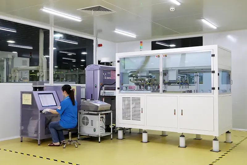
Automated Optical Inspection (AOI): High-speed, high-precision visual inspection of all inner and outer circuit layers to detect minute defects.
Electrical Test (E-Test): 100% electrical testing to verify circuit continuity and isolation, ensuring every connection functions as designed.
X-Ray Inspection: Used to verify internal layer registration, microvia alignment, and solder joint quality, especially critical for complex HDI stack-ups.
Impedance Control Testing: Precise impedance measurement and control to guarantee signal integrity and high-frequency performance.
Material Verification: All incoming base materials and chemicals are thoroughly inspected to ensure they meet our strict quality standards.
Industry Certifications: Our adherence to ISO9001, IATF16949 (Automotive standard), ISO14001 (Environmental), and UL certifications underscores our dedication to consistent quality, responsible manufacturing, and product safety.
Your Strategic Partner in HDI PCB Manufacturing: Why TriWin?
Choosing TriWin means partnering with an experienced HDI PCB manufacturer dedicated to delivering exceptional quality and performance for your most complex and innovative designs.
Advanced Manufacturing Capabilities: Our facilities are equipped with state-of-the-art laser drilling machines, advanced lamination presses, and high-precision etching equipment specifically optimized for HDI PCB fabrication, ensuring precise microvia formation and accurate layer alignment.
Expert Engineering Support: TriWin’s professional engineering team offers extensive experience in HDI PCB design for manufacturability (DFM). We provide crucial technical support and guidance to optimize your designs for performance, cost-efficiency, and successful production.
Flexible HDI Stack-up Solutions: We offer a versatile range of HDI stack-up types (e.g., 1+N+1, 2+N+2, Any-Layer HDI) to meet diverse design complexities, balancing performance, cost, and manufacturability for your specific application.
Premium Material Sourcing: We utilize high-quality base materials from trusted global suppliers, including various TG laminates, halogen-free options, and specialized low-loss high-frequency materials, ensuring the optimal foundation for your HDI boards.
Commitment to Quality: Our rigorous quality control processes and comprehensive testing ensure every HDI PCB meets the highest standards of reliability and functionality, from prototype to volume production.
