As a leader in the printed circuit board industry, we at Tri-Win Circuits often encounter questions that delve into the specifics of our manufacturing process. One of the most common points of confusion is the distinction between creating a circuit board and populating it with components. A frequent query we hear is, “Do you, as a PCB fabricator, solder on the surface mount transistors and other parts?”
- What is the Fundamental Role of a PCB Fabricator?
- So, Who Is Responsible for Soldering the Transistors?
- How Are Surface Mount Transistors Actually Soldered? The SMT Assembly Process
- Why Is This Two-Step Process (Fabrication & Assembly) So Crucial
- Can a Single Company Handle Both PCB Fabrication and Assembly?
- Tri-Win Circuits: Your Partner from Bare Board to Fully Assembled PCB
The short and direct answer is: No, a PCB fabricator does not typically solder components. That crucial step belongs to a distinct, yet closely related, process known as PCB Assembly (PCBA).
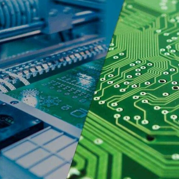
This distinction is fundamental to understanding the electronics supply chain. While we are experts in both, separating these two stages—fabrication and assembly—is key to achieving the precision, quality, and efficiency modern electronics demand. Let’s explore the roles of each process and clarify who is responsible for soldering those vital surface mount transistors onto your board.
What is the Fundamental Role of a PCB Fabricator?
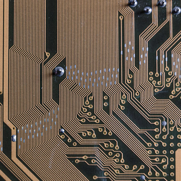
Think of a PCB fabricator as the builder of a high-tech foundation. Our primary role is to manufacture the bare, unpopulated printed circuit board according to a customer’s specific design files (like Gerber files). This intricate process transforms raw materials into a custom-engineered platform, ready to host an entire ecosystem of electronic components.
The fabrication process itself involves a series of sophisticated steps:
- Material Selection: We start with a base laminate material, such as FR-4, Rogers, or a metal core for thermal management, depending on the application’s requirements.
- Circuit Patterning & Etching: We transfer the circuit design onto copper-clad layers and chemically etch away the unwanted copper, leaving only the conductive traces, pads, and planes.
- Layer Lamination: For multi-layer PCBs, we press these individual layers together with insulating material under high temperature and pressure to form a single, robust board.
- Drilling: Precision holes, known as vias, are drilled to connect different layers of the board electronically.
- Plating: A thin layer of copper is deposited in the drilled holes to create the electrical connections (plated-through holes).
- Solder Mask & Silkscreen: We apply a protective solder mask (typically green, blue, or red) to insulate the copper traces, leaving only the pads exposed for soldering. Finally, a silkscreen layer is printed to indicate component placement, part numbers, and other essential markers.
At the end of this journey, the product is a pristine, high-quality bare PCB. It has all the necessary copper pads where transistors will eventually sit, but it is entirely free of components.
So, Who Is Responsible for Soldering the Transistors?
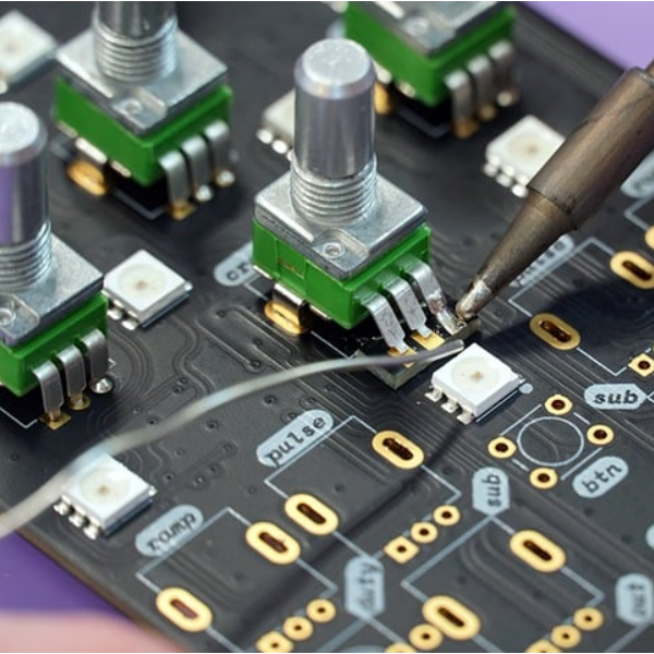
This is where PCB Assembly (PCBA) comes into play. The responsibility for accurately placing and permanently soldering surface mount transistors, resistors, capacitors, and integrated circuits onto the board falls to the PCB assembler.
At Tri-Win Circuits, we offer this as a core service, transitioning seamlessly from fabrication to assembly to provide a complete, one-stop solution for our clients. The PCBA process uses a highly automated and precise methodology called Surface Mount Technology (SMT) for components like modern transistors.
How Are Surface Mount Transistors Actually Soldered? The SMT Assembly Process
Soldering tiny surface mount components is not a manual task performed by fabricators; it’s a high-tech assembly line process designed for speed and reliability. Here’s a simplified breakdown of how we get it done:
- Solder Paste Application: A stainless-steel stencil, which is a template of the PCB’s pads, is laid over the board. A machine then uses a squeegee to apply a precise amount of solder paste onto each exposed pad. This paste is a mixture of tiny solder spheres and flux.
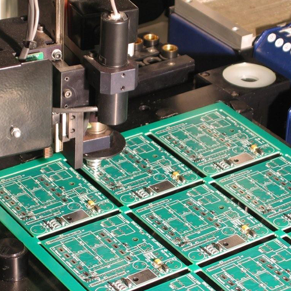
- Component Placement: The board moves to a “Pick-and-Place” machine. This robotic marvel uses vacuum nozzles to pick components—including surface mount transistors—from reels and trays and places them onto their corresponding pads on the solder paste with incredible speed and accuracy. The sticky nature of the paste holds the components in place temporarily.
- Reflow Soldering: The board, now populated with components, travels through a long reflow oven with multiple heating zones. The temperature is carefully controlled to first activate the flux and then melt the solder, forming strong and permanent electrical and mechanical bonds between the components and the PCB pads. As the board cools, the solder solidifies.
- Inspection: Quality is paramount. After reflow, the assembled boards undergo rigorous inspection. Automated Optical Inspection (AOI) machines scan the boards to check for placement accuracy, solder joint quality, and other potential defects. For complex components like BGAs, we use X-ray inspection to see hidden solder joints.
This entire process ensures that every transistor and component is soldered with consistency and quality that would be impossible to achieve in the fabrication stage.
Why Is This Two-Step Process (Fabrication & Assembly) So Crucial?
Separating PCB fabrication from assembly is a matter of specialization and efficiency. Each process requires entirely different equipment, expertise, chemical processes, and quality control metrics.
- Specialized Expertise: Fabricators are experts in materials science, lamination, and chemical etching. Assemblers are experts in automation, soldering science, and component logistics.
- Quality Control: By separating the stages, we can perform dedicated quality checks on the bare board before any value is added by placing expensive components. This prevents flawed boards from entering the assembly line.
- Process Optimization: The machinery and environment for creating a bare board (a wet, chemical-heavy process) are completely different from the clean, highly-automated environment needed for placing and soldering sensitive electronics.
Can a Single Company Handle Both PCB Fabrication and Assembly?
Yes, and this is where a “turnkey” provider like Tri-Win Circuits offers a significant advantage. While the processes are distinct, having a single partner manage both eliminates communication gaps, streamlines logistics, and ensures total accountability. This integrated approach is the most efficient path from concept to a fully functional electronic product.
Here’s how a turnkey solution compares to using separate vendors:
| Aspect | Turnkey Solution (Tri-Win Circuits) | Using Separate Vendors |
|---|---|---|
| Supply Chain | Simplified. One point of contact for the entire process, from bare board to final assembly. | Complex. You manage multiple suppliers, shipments, and timelines. |
| Accountability | Total. A single partner is responsible for the final product’s quality and functionality. | Divided. Fabrication and assembly vendors may blame each other for issues. |
| Lead Time | Reduced. No delays from shipping boards between facilities or coordinating schedules. | Longer. Includes transit time and potential scheduling conflicts between vendors. |
| Technical Support | Holistic. Our engineers understand the interplay between fabrication and assembly for optimal results. | Siloed. Each vendor only provides support for their specific part of the process. |
Tri-Win Circuits: Your Partner from Bare Board to Fully Assembled PCB
In conclusion, while the PCB fabricator masterfully creates the board itself, it is the PCB assembler who expertly solders on the surface mount transistors and brings your design to life. Understanding this distinction is key to navigating the world of electronics manufacturing.
At Tri-Win Circuits, we pride ourselves on mastering both domains. Our integrated fabrication and assembly services provide a seamless, reliable, and efficient solution for projects ranging from quick-turn prototypes to large-scale production. By handling your entire project under one roof, we ensure that every trace on the board and every solder joint on a transistor is executed to perfection. Ready to turn your design into a reality? Contact us today to get started.

