Ceramic PCBs: Advanced Solutions for Extreme Performance
At TriWin Circuits, we specialize in Ceramic PCBs, providing advanced solutions for demanding electronic applications. Our boards, built on ceramic substrates, offer superior thermal conductivity, excellent electrical insulation, and stable high-frequency performance. They’re designed to withstand extreme temperatures and harsh environments, making them suitable for high-power, high-frequency, and high-reliability designs. Learn how TriWin’s expertise in ceramic PCB manufacturing can support your project needs.
What Makes Ceramic PCBs Unique?
Ceramic PCBs differ fundamentally from conventional FR-4 (organic) and even Metal Core PCBs like aluminum or copper base. Their unique capabilities stem from the inherent properties of the ceramic materials themselves and the specialized manufacturing processes, which often involve direct bonding of copper without adhesives for an exceptionally efficient thermal path.
Key properties that define ceramic PCBs include:
Exceptional Thermal Conductivity: Ceramic materials, such as Alumina (Al2O3) and Aluminum Nitride (AlN), boast significantly higher thermal conductivity compared to traditional PCB substrates. Alumina (96%) offers good thermal performance (e.g., 24 W/m·K), while Aluminum Nitride (AlN) provides outstanding conductivity (e.g., 170-200 W/m·K), vital for effective heat dissipation in high-power applications.
Excellent Electrical Insulation (High Dielectric Strength): Ceramic provides superior electrical insulation and high dielectric strength, crucial for preventing current leakage and maintaining signal integrity, particularly in high-voltage circuits.
Low Thermal Expansion Coefficient (CTE): The CTE of ceramic closely matches that of silicon chips. This minimizes thermal stress on soldered joints and components during temperature fluctuations, significantly improving reliability and extending product lifespan in thermal cycling environments.
High Temperature Resistance: Ceramic PCBs can operate reliably across extreme temperature ranges, typically from -55°C to over 350°C, far surpassing the limitations of organic PCB materials.
Stable High-Frequency Performance: With low dielectric loss (Df) and a stable dielectric constant (Dk), ceramic PCBs ensure minimal signal attenuation and distortion. This makes them ideal for sensitive high-frequency, RF, and Microwave applications.
Chemical Resistance: Ceramic materials are largely inert and highly resistant to most chemicals, ensuring durability and long-term stability in corrosive or harsh chemical environments.

PCB manufacturing
TriWin's Range of Ceramic PCB Solutions
TriWin Circuits provides diverse ceramic PCB solutions, each manufactured with precision to suit specific application requirements and performance needs:
High-Temperature Co-fired Ceramic (HTCC):
- Process: Conductive traces are screen-printed onto ceramic layers, then co-fired at extremely high temperatures (around 1600°C) to form a dense, monolithic structure.
- Characteristics: Known for exceptional robustness, excellent thermal and electrical properties, and capability for complex multi-layer designs with embedded components.
- Typical Uses: High-power modules, extreme environment sensors, automotive electronics.
Low-Temperature Co-fired Ceramic (LTCC):
- Process: Ceramic layers with conductive pastes are co-fired at lower temperatures (around 850°C), enabling integration with various passive components (resistors, capacitors, inductors).
- Characteristics: Offers finer lines, improved precision, and suitability for creating highly integrated modules.
- Typical Uses: RF modules, medical devices, integrated circuits, wireless communication systems.
Thick Film Ceramic PCB:
- Process: Conductive, resistive, and dielectric pastes are screen-printed onto a finished ceramic substrate (often Alumina) and then fired at moderate temperatures.
- Characteristics: A cost-effective solution for certain applications, suitable for integrated resistors and simpler circuitry.
- Typical Uses: General electronics, automotive sensors, heating elements.
Low-Temperature Co-fired Ceramic (LTCC):
- Process: Conductive layers are deposited onto the ceramic substrate using advanced techniques like sputtering or plating.
- Characteristics: Provides very high precision, finer lines and spaces (down to micrometers), and superior electrical performance for critical signal integrity.
- Typical Uses: High-frequency components, optical devices, micro-sensors, advanced IC packaging.
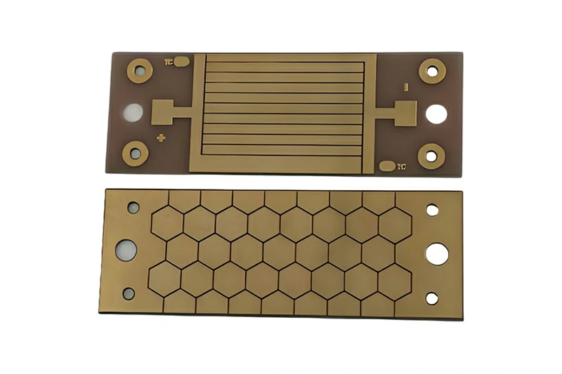
Direct Copper Bonded (DCB) Ceramic PCB:
- Process: Thick copper foils are directly bonded to the ceramic substrate (typically Alumina or AlN) at high temperatures, without an adhesive layer.
- Characteristics: Offers outstanding thermal conductivity and high power handling capability due to the adhesive-free, direct thermal path, making it highly efficient.
- Typical Uses: High-power LEDs, IGBT power modules, high-current rectifiers, automotive power electronics.
Key Advantages of TriWin Ceramic PCBs
TriWin’s Ceramic PCBs offer distinct advantages, crucial for the most advanced electronic designs
Extreme Thermal Management
Our ceramic substrates provide unmatched heat dissipation efficiency, directly contributing to cooler operation and extended life for high-power components.
Superior Electrical & High-Frequency Performance
With excellent dielectric properties and low loss, TriWin's ceramic PCBs ensure minimal signal attenuation and distortion, making them ideal for sensitive RF, microwave, and high-speed digital circuits.
Unparalleled Reliability in Harsh Environments
Ceramic's inherent resistance to high temperatures, thermal shock, chemicals, and mechanical stress ensures consistent and long-term reliability where other PCB types would typically fail.
Compact & Miniaturized Designs
The efficient heat removal capabilities and potential for embedded components in co-fired ceramics allow for higher power densities within smaller footprints, facilitating compact and miniaturized electronic designs.
Extended Product Lifespan
The combined benefits of superior thermal management, robust material properties, and excellent CTE matching directly translate into significantly extended product lifespans for devices utilizing TriWin's ceramic PCBs.
TriWin's Ceramic PCB Manufacturing Capabilities & Specifications
TriWin Circuits is equipped with specialized capabilities to produce high-quality Ceramic PCBs tailored to your project’s precise requirements.

| Parameter | Specification (Customizable) | |||||
| Base Ceramic Materials | Alumina (Al2O3) 96%, Alumina (Al2O3) 99%, Aluminum Nitride (AlN) | |||||
| Layers | 1 Layer, 2 Layers (DCB, Thick/Thin Film); Multilayer (HTCC, LTCC – up to [Specify your max layers, e.g., 20+]) | |||||
| Board Thickness | 0.25 mm to 3.0 mm (varies by ceramic type and layer count) | |||||
| Copper Thickness/Weight | DCB: 0.1 mm to 0.8 mm; Thick Film: 10 μm to 30 μm; Thin Film: 1 μm to 10 μm | |||||
| Minimum Line Width/Spacing | DCB: 100/100 μm; Thick Film: 100/100 μm; Thin Film: 25/25 μm (technology dependent) | |||||
| Minimum Hole/Via Size | Laser Drilled: Down to 50 μm; Mechanically Drilled: Varies | |||||
| Surface Finishes | Gold Plating (Ni/Au), Silver, Platinum, Palladium, Solderable Pads | |||||
| Thermal Conductivity | Alumina: 20-28 W/m·K; AlN: 170-200 W/m·K (for ceramic substrate itself) | |||||
| Operating Temperature Range | -55°C to >350°C (depending on specific ceramic and application) | |||||
| CTE (Coefficient of Thermal Expansion) | Alumina: ~6-7 ppm/°C, AlN: ~4.5 ppm/°C (matches silicon) | |||||
| Certifications | UL, ISO9001, IATF16949, ISO14001 | |||||
| Special Processes | Precision Laser Machining, Via Filling, Fine Line Pattern Plating, Direct Copper Bonding | |||||
Designing for Success: Ceramic PCB Guidelines
For engineers designing with ceramic PCBs, considering these guidelines can optimize performance and manufacturability:
Material Selection: Carefully choose between Alumina (cost-effective, good thermal) and Aluminum Nitride (AlN) (superior thermal, higher cost) based on your specific thermal dissipation, electrical, and budget requirements.
CTE Matching: Prioritize matching the Coefficient of Thermal Expansion (CTE) of the ceramic substrate with that of the attached components (especially silicon chips) to minimize stress during thermal cycling and enhance long-term reliability.
Via/Hole Considerations: For high-density designs, utilize laser drilling for very small and precise vias. Discuss filled vias with TriWin for improved thermal performance and signal integrity.
Conductor Material & Thickness: For high-frequency applications, gold plating is often preferred. Consider the thickness of the conductor layer based on current handling and precision needs (Thin Film for very fine lines, Thick Film or DCB for higher currents).
Layer Count & Stack-up: For HTCC and LTCC multi-layer designs, collaborate with TriWin on optimal stack-up to meet complex electrical performance and thermal management goals.
Thermal Management Strategies: While the ceramic itself is an excellent heat sink, consider supplementary thermal vias or integrated heat spreading features for extreme power dissipation requirements.
Surface Finish Selection: Choose a surface finish (e.g., Ni/Au plating) compatible with ceramic materials and your intended assembly process (e.g., wire bonding, soldering).

Your Strategic Partner in Ceramic PCB Manufacturing: Why TriWin?
Choosing TriWin means partnering with a specialist in Ceramic PCB manufacturing, dedicated to delivering the highest standards of quality and performance for your critical applications.
Specialized Expertise: We possess a deep understanding of ceramic materials and complex ceramic PCB fabrication processes, enabling us to tackle the most challenging designs with precision.
Advanced Fabrication Technologies: Our state-of-the-art facilities are equipped with specialized machinery for ceramic manufacturing, including precision laser drilling, high-temperature co-firing capabilities, and Direct Copper Bonding (DCB) techniques, ensuring superior accuracy and performance.
Uncompromising Precision & Reliability: We emphasize tight tolerances and co
nsistent quality critical for ceramic PCBs, ensuring optimal thermal and electrical performance over time.
Comprehensive Quality Assurance: Every ceramic PCB undergoes rigorous testing, including AOI, electrical testing, and X-ray inspection, to guarantee reliability and adherence to specifications.
Diverse Material Sourcing: We work with various high-quality ceramic substrates (Alumina, AlN) to provide the best material solution for your project’s specific thermal and electrical requirements.
Industry Certifications: Our adherence to ISO9001, IATF16949 (Automotive standard), ISO14001 (Environmental), and UL certifications underscores our commitment to quality, responsible manufacturing, and product safety.
