I. Introduction: Why HDI PCBs are Essential Today
The demand for smaller, lighter, and more functional electronic devices is constantly growing. Products from smartphones and wearables to advanced medical and automotive systems require increasing complexity in shrinking spaces. This trend necessitates advanced PCB technology capable of higher component density and improved performance than traditional methods.
High-Density Interconnect (HDI) PCBs are the solution. They allow more circuitry on a smaller board area using microvias, fine lines, and advanced layering. HDI technology isn’t just about size; it also enhances performance with better signal integrity, less EMI, and increased reliability for demanding applications. This guide covers the key principles, rules, and practices for successful HDI PCB design.
II. What Defines an HDI PCB?
An HDI PCB features significantly higher wiring density per unit area compared to standard PCBs. Key characteristics, often defined by standards like IPC-2226, include:
- Microvias: Small drilled holes, typically 150 µm or less in diameter, usually created with lasers.
- Fine Lines & Spaces: Conductive traces and the gaps between them are very narrow, often 100 µm (4 mils) or less.
- Small Capture Pads: The pads around vias are smaller, typically 400 µm (16 mils) or less.
- High Pad Density: A greater concentration of component connection pads per square centimeter.
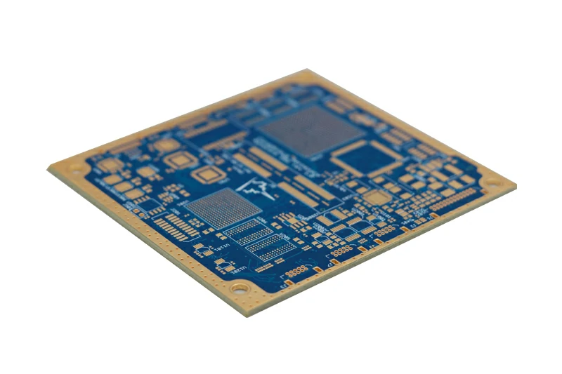
These features differentiate HDI from conventional PCBs, which rely more on larger through-hole vias. The ability to create vias that only connect specific layers (microvias) dramatically increases the available routing space, especially under fine-pitch components like BGAs, enabling denser designs not possible otherwise.
III. Core Technologies Enabling HDI
Microvias are fundamental to HDI technology. Their small size allows for more connections in a smaller area. Different types of microvias provide routing flexibility:
- Blind Vias: Connect an outer layer to an inner layer without going through the entire board.
- Buried Vias: Connect only inner layers, hidden within the board structure.
- Stacked Vias: Microvias placed directly atop each other across multiple layers, requiring specialized filling and plating.
- Staggered Vias: Microvias offset on different layers, using more space but potentially simpler to manufacture than stacked.
- ELIC (Every Layer Interconnect): Stacked microvias connecting every adjacent layer for maximum density and routing freedom.
Laser drilling is the primary method for creating these small microvias. Via-in-Pad (VIP) technology, placing a via directly in a component’s solder pad, is critical for routing fine-pitch BGAs and requires reliable via filling and capping.
Layer Stack-Up Strategies: Strategic layer stack-up is vital for HDI, affecting routing density, signal integrity, and manufacturability. HDI boards use sequential lamination, adding layers or sub-laminates in stages with intermediate drilling and plating. Common stack-ups are noted as X+N+X, where X indicates the number of sequential build-up layers on each side of a core (e.g., 1+N+1, 2+N+2).
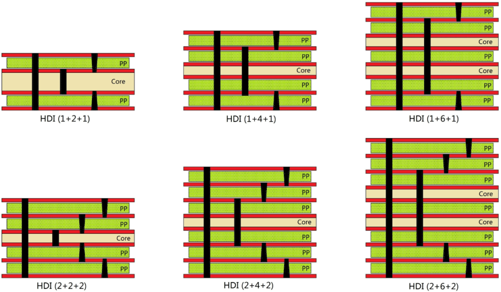
Effective stack-up design involves minimizing layers while meeting routing needs, placing signal layers next to solid reference planes (ground/power), using thin dielectrics for impedance control and manageable microvia aspect ratios, and ensuring symmetry to prevent warping.
IV. Essential Design Rules and Guidelines for HDI
Designing an HDI PCB demands strict adherence to specific rules, which are much tighter than for conventional boards. The most critical first step is always collaborating closely with your PCB manufacturer. Obtain their detailed Design for Manufacturability (DFM) specifications early, as their precise capabilities define your design limits.
Key design considerations and rules include:
- Trace Width and Spacing: These are much finer (e.g., 75 µm / 75 µm or 3 mil / 3 mil is common, potentially smaller). Ensure your manufacturer can reliably produce the required minimums. These dimensions directly influence signal impedance and current capacity.
- Vias and Annular Rings: Microvia diameters are small (e.g., 100 µm – 150 µm). The aspect ratio (drilled depth to diameter) is crucial for plating quality; laser microvias typically have low aspect ratios (e.g., ≤ 1:1), limiting single microvias to one or two layers depending on thickness. Capture pad size must provide a sufficient annular ring for reliable connections. Via spacing is also tighter in HDI.
- Component Placement: Optimize placement, especially for fine-pitch BGAs and other high-density components, to facilitate routing. Consider manufacturer requirements for via-in-pad filling and capping if used, as proper surface planarity is needed for soldering reliability.
- Clearances: Maintain strict clearances from traces, pads, and vias to other copper features and the board edge, adhering to manufacturer specifications to prevent shorts or manufacturing defects.
Designing strictly within your manufacturer’s documented capabilities is the most important rule for ensuring a successful HDI board.
V. Managing Signal and Power Integrity in HDI
High-speed signals, dense routing, and small features make Signal Integrity (SI) and Power Integrity (PI) complex challenges in HDI design.
Signal Integrity (SI): Maintaining signal quality is critical. Controlled impedance traces are often necessary for high-speed signals to prevent reflections; this requires precise control over trace dimensions and dielectric properties based on the stack-up. Routing strategies like keeping traces short, avoiding sharp bends, matching lengths for differential pairs, and minimizing via stubs are vital.
Solid ground and power planes are essential reference planes for signal return paths, providing low impedance. Routing signals adjacent to these planes and ensuring continuous return paths help reduce signal degradation and crosstalk. Avoiding routing high-speed signals over plane splits is also crucial. Techniques like placing traces at right angles or using ground traces help mitigate crosstalk.
Power Integrity (PI): Ensuring a stable power supply is equally important in dense designs. Decoupling capacitors, placed very close to IC power pins, are used to filter high-frequency noise and provide local charge storage. Using multiple capacitor values addresses noise across different frequency ranges.
Solid power and ground planes minimize the impedance of the power distribution network (PDN), reducing voltage drop and noise. Via stitching is used to connect ground planes on different layers, further lowering impedance and providing multiple return paths for improved PI. Advanced SI/PI analysis tools should be used to simulate and verify performance early in the design cycle.
VI. Thermal Management in Dense HDI Layouts
Effective heat dissipation is challenging in HDI boards because components are packed more densely, leaving less space for traditional cooling features. This concentration of heat can negatively impact performance and component lifespan.

Strategies to manage heat in HDI designs include:
- Thermal Vias: Using vias, particularly under hot components, to conduct heat away. Via-in-pad technology with thermal filling is highly effective for transferring heat from component pads to inner planes or heatsinks.
- Copper Areas: Utilizing large copper pours or planes connected to thermal structures (like ground planes) to spread heat across the board area.
- Material Choice: Considering substrate materials with higher thermal conductivity if required, or using thermally conductive via fill materials.
- Component Placement: Arranging high-power components strategically to maximize heat dissipation efficiency and ensure temperature-sensitive components are located away from heat sources.
- Thermal Analysis: Performing thermal simulations early in the design process helps identify potential hotspots and validate the thermal management approach.
Incorporating thermal considerations from the initial design phase is essential for the reliability of dense HDI boards.
VII. Design for Manufacturability (DFM) is Crucial for HDI
For HDI PCBs, Design for Manufacturability (DFM) is not just a recommendation; it is a necessity. The fine features, tight tolerances, and complex sequential build processes make fabrication highly sensitive. Design errors can be very costly and delay production significantly.
Key DFM considerations for HDI include:
- Strict Adherence to Manufacturer Specs: Always design within your fabricator’s documented limits for trace/space, via sizes, aspect ratios, drill clearances, and lamination capabilities.
- Via Filling and Capping: Understand and follow the manufacturer’s specific requirements for filling microvias (especially via-in-pad) and capping them with copper plating to create a planar surface required for reliable component soldering.
- Solder Mask & Silkscreen: Ensure correct clearances for solder mask dams between fine-pitch pads to prevent solder bridging. Silkscreen should not encroach on solderable surfaces.
- Copper Balancing: Design the stack-up to ensure a reasonably balanced distribution of copper on each layer and symmetry across the board structure. This helps prevent warping or twist during manufacturing and thermal cycles.
- Panelization: Consider how the individual boards will be fabricated on a larger panel to optimize material usage and process efficiency.
Early and continuous collaboration with your chosen HDI manufacturer is critical. Engage with them from the initial design stages to discuss stack-up options, review design rules, and ideally, get a DFM check on your design files before committing to production.
VIII. Utilizing Advanced Design Tools
Designing complex HDI PCBs requires sophisticated PCB design software (CAD tools) equipped with specialized features. Attempting HDI layout with basic tools is impractical and risky.
Essential capabilities in CAD tools for HDI design include:
- Advanced Stack-up Editors: For precise definition of layers, materials, thicknesses, and the sequential lamination process, crucial for impedance calculations.
- Microvia Management: Tools to define, place, and manage different microvia types, their aspect ratios, drilling methods (laser), and filling requirements.
- Robust Design Rule Checking (DRC): A powerful engine capable of enforcing fine-pitch tolerances, complex via rules, and clearances specific to HDI designs.
- Integrated Analysis Tools: Features for calculating impedance and performing Signal Integrity (SI), Power Integrity (PI), and Thermal simulations to verify design performance before manufacturing.
- Advanced Routing Features: Tools optimized for routing in dense areas, handling differential pairs, minimizing stub lengths, and supporting complex via patterns (like BGA fanouts).
- 3D Visualization: Helps designers visualize the complex multi-layer structure and component placement in three dimensions.
Leveraging these advanced tools, combined with simulation and thorough DFM checks, is crucial for successful first-pass HDI designs.
IX. Conclusion: Mastering HDI for Future Electronics
High-Density Interconnect (HDI) PCB technology is indispensable for developing the compact, high-performance electronic devices driving innovation today. While it introduces complexities beyond standard PCB design, the benefits in miniaturization, electrical performance, and reliability are significant.
Successful HDI design hinges on a deep understanding of microvias, strategic stack-up planning, meticulous adherence to fine-pitch design rules, and careful attention to SI, PI, and thermal management. Above all, close collaboration with a capable HDI PCB manufacturer is essential. By mastering these aspects and partnering with an experienced fabricator, designers can effectively navigate the challenges of HDI and unlock the full potential of their next-generation products.
As a professional PCB manufacturer specializing in multilayer, HDI, flexible, rigid-flex, high-frequency, and metal base PCBs for demanding applications like automotive, industrial, and medical fields, TriWin PCB possesses the expertise and advanced equipment necessary to help turn your complex, high-density designs into reliable finished products.
X. Frequently Asked Questions (FAQs)
- What are the defining features of an HDI PCB? Microvias (≤ 150 µm), fine lines/spaces (≤ 100 µm), small capture pads, and high connection density.
- What is a microvia aspect ratio? The ratio of its drilled depth to its diameter, critical for ensuring reliable plating inside the via.
- When might I need an HDI PCB? When your design requires higher component density, smaller board size, improved electrical performance for high-speed signals, or enhanced reliability in demanding environments.
- What are the most common HDI stack-up types? 1+N+1 and 2+N+2 are common, representing the number of sequential build-up layers on each side of a core.
- Why is DFM particularly important for HDI? The fine features and complex processes make HDI fabrication highly sensitive to design tolerances, making errors costly if not caught early.
- What IPC standard covers HDI PCBs? IPC-2226 is the relevant standard.
Designing with HDI enables the innovation required for today’s advanced electronics.


