Few things in the electronics world are more fundamental than circuit board patterns. These intricate networks of copper traces dictate how signals flow between components on printed circuit boards (PCBs). Everything—from a simple calculator to advanced aerospace systems—relies on precisely arranged copper paths to enable a device to function. In this article, we will explore the importance of circuit board patterns, delve into their types, address design challenges, and discuss how a reliable manufacturing partner can help turn intricate schematics into dependable hardware.
Understanding Circuit Board Patterns
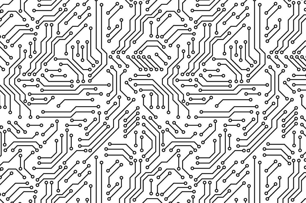
Printed circuit boards are essentially layered sandwiches of conductive and insulating materials. The metal traces, or circuits, that appear on these boards have one main purpose: to connect different electronic components and facilitate the flow of electricity or data signals from one part of the circuit to another. Circuit board patterns, therefore, not only define the physical layout of these tracks but also influence characteristics such as signal integrity, interference levels, and overall reliability.
A circuit board pattern is more than just “paths” on a copper layer. It represents a meticulous arrangement born from rigorous engineering calculations, ensuring that every data lane, power line, and ground reference is placed optimally. Designers must consider current load, voltage levels, electromagnetic compatibility, and thermal dynamics to decide how each copper segment is routed.
Types of Circuit Board Patterns
Single-Layer Patterns
Single-layer boards allow all copper traces to exist on only one side of the substrate. Typically found in basic consumer electronics, such as remote controls and simple toys, these circuit boards use straightforward patterns, enabling components to be placed and soldered on the same side. They are cost-effective to produce but are limited in terms of routing flexibility.
Double-Sided Patterns
Double-sided circuit boards add another copper layer on the reverse side of the substrate. Traces can now cross over each other on opposite sides, effectively doubling available routing space. Via holes, drilled through the board, provide connections between the top and bottom layers. This added flexibility allows for more complex circuit arrangements and can support slightly higher component density.
Multilayer and HDI Patterns
More advanced products make use of multilayer boards, where multiple copper layers are sandwiched with insulating material. These boards can have anywhere from four to dozens of layers, thereby creating complex patterns suitable for high-density interconnect (HDI) designs. HDI boards frequently utilize micro vias and buried vias to minimize space while maximizing interconnect capacity. Modern smartphones, network routers, and aerospace systems often rely on high-layer-count boards with carefully orchestrated circuit board patterns for optimum performance.
Flexible vs. Rigid Board Patterns
Flexible circuit boards (Flex PCBs) and rigid-flex boards draw renewed attention to the importance of pattern layout. Unlike traditional rigid boards, flex PCBs use bendable substrates that can conform to curved or non-flat assemblies. Hence, the circuit board patterns must account not just for conductivity but also for stress, bending radius, and repeated mechanical flexing without fracturing.
Design and Layout Considerations
When developing circuit board patterns, engineering decisions around copper thickness, material layers, and track geometry all play enormous roles in functionality and reliability.
- Copper Thickness and Dielectric Requirements: Thicker copper supports higher current flow. However, it also demands more spacing between traces and around vias, which may reduce the available routing area.
- Spacing, Track Width, and Clearance: To avoid unintended shorts or crosstalk, design rules specify minimal distances between conductive paths. These rules become more stringent at higher signal frequencies.
- Signal Integrity and EMC Compliance: Circuit board patterns for high-speed digital or analog signals must ensure minimal interference. Routing lines in differential pairs, maintaining consistent impedance, and including proper ground planes can all reduce noise and electromagnetic emissions.
Impact of Patterns on Performance
Current Capacity and Heat Dissipation
The width and thickness of circuit paths determine how much current they can carry without excessive heating. Overloaded traces can overheat and damage neighboring components, making proper pattern design vital for stable performance.
Minimizing Noise and Interference
Modern electronics often incorporate sensitive analog sensors or high-speed digital interfaces. Poorly optimized patterns can lead to electromagnetic interference (EMI), cross talk, and other signal degradation issues. By carefully placing ground return paths and maintaining appropriate spacing, engineers can reduce noise while boosting signal clarity.
High-Speed Signal Routing and Data Integrity
Circuit board patterns become more complex at higher data rates. For instance, high-speed DDR or PCIe signals require strict impedance control and minimal stubs. Skew matching might become necessary so that all signals in a data bus arrive at the receiving device simultaneously, ensuring reliable data transfers without errors.

Manufacturing Techniques and Pattern Precision
Producing consistent, high-precision circuit board patterns calls for meticulous processes across multiple steps:
- Photolithography: A photosensitive mask defines where copper is etched or retained. A misalignment here can produce broken or bridged traces.
- Etching: Chemical etching removes unwanted copper, leaving only the needed conductive paths. Controlled etch rates are crucial to replicating the intended circuit patterns.
- Drilling, Plating, and Finishing: Vias connect different layers using electroplating, and surface finishes (such as HASL, ENIG, or immersion tin) protect the copper from oxidation and ensure reliable soldering.
Ensuring repeatability at scale can be challenging, particularly for boards featuring narrow line widths and fine-pitch components. Automated optical inspection (AOI) and other quality control measures detect manufacturing defects early, helping maintain consistent quality across large production runs.
Common Challenges and Solutions
Circuit board patterns can be thrown off by temperature fluctuations, mechanical stresses, or even the inherent tolerances of the manufacturing equipment. Overcoming trace misalignment, controlling impedance in high-speed designs, and preventing warpage in boards with many layers all require specialized knowledge. High-end PCB manufacturers invest heavily in advanced machinery and tightly controlled environments to mitigate these risks.
In addition, engineers often use design software that integrates electrical and thermal simulation tools. By testing the circuit board pattern in a virtual environment, they can detect potential hotspots, interference, or excessive voltage drops long before they fabricate the prototype.
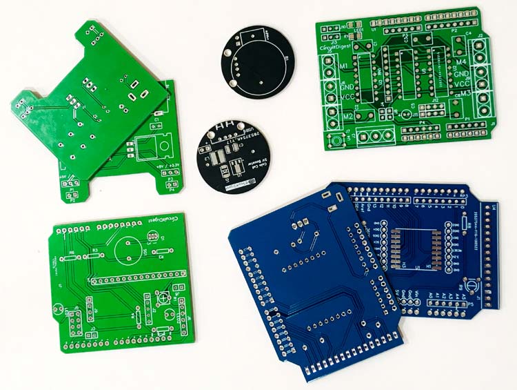
Applications of Various Circuit Board Patterns
Circuit board patterns differ significantly depending on the target sector:
- Consumer Electronics: Devices like smartphones, laptops, and gaming consoles rely on dense, multilayer designs optimized for both performance and compact size.
- Automotive and Industrial Systems: Harsh environments with temperature extremes and vibrations require robust boards with thick copper layers and reliable interconnections.
- Medical Devices: From wearable health monitors to complex imaging systems, precision and reliability matter above all. Circuit board patterns must be validated to meet stringent safety standards.
Conclusion and Next Steps
Circuit board patterns lie at the foundation of electronic innovation. By optimizing trace width, layer configurations, and design rules, engineers maximize device reliability, performance, and longevity. For complex applications—be it high-speed data processing, heavy industrial usage, or intricate flexibility demands—expert knowledge and advanced manufacturing processes are crucial.
At TriWin, we offer a broad spectrum of PCB manufacturing services, including single-layer, double-sided, multilayer, and metal-based options. Our extensive experience with advanced technologies such as HDI and flexible boards ensures that the layout of your circuit board patterns is handled with precision. Backed by ISO9001, IATF16949, ISO14001, and UL certifications, our team is well-prepared to deliver boards that match your specific requirements. We are proud to guide you through every step, from the initial concept phase to full-scale production, ensuring your next project meets the demands of modern electronics while maintaining high quality and reliability.


