High-frequency PCB communication circuits are at the heart of modern electronics, enabling fast, reliable data transfer in applications like telecommunications, radar systems, automotive radar, and high-speed computing. Designing and manufacturing these circuits require specialized knowledge, advanced materials, and cutting-edge equipment to ensure signal integrity and performance. In this guide, we’ll explore what high-frequency PCBs are, their key design considerations, applications, and manufacturing challenges, providing actionable insights for engineers and businesses alike.
What Are High Frequency PCB Communication Circuits?
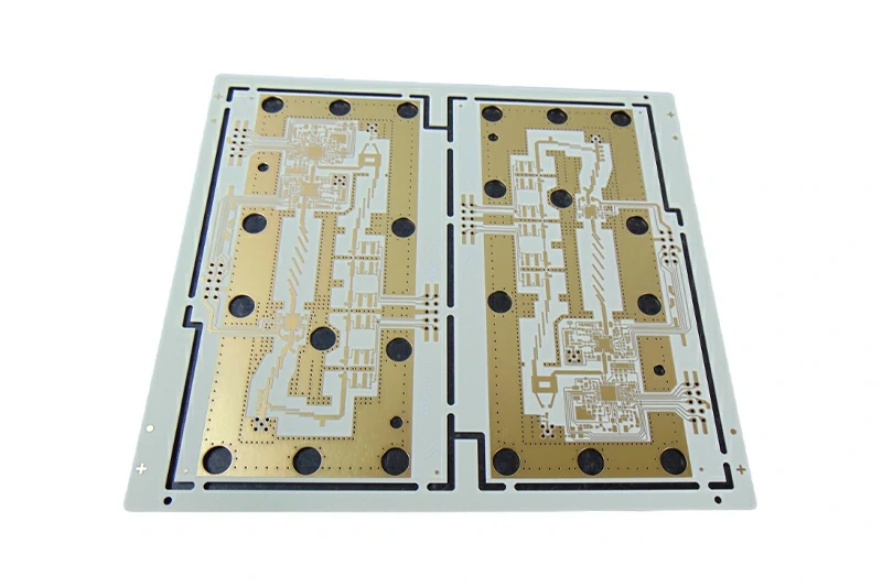
High-frequency PCBs are printed circuit boards designed to operate at frequencies typically above 1 GHz, where signal integrity becomes critical. These boards are essential for communication circuits that transmit and receive high-speed signals with minimal loss or interference. Unlike standard PCBs, high-frequency boards use specialized materials and layouts to manage electromagnetic waves, impedance, and heat dissipation effectively.
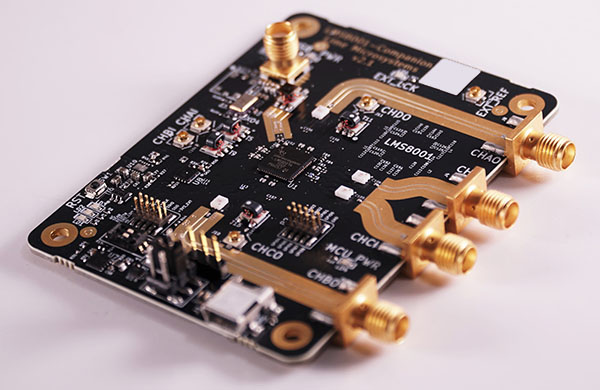
In communication systems, these PCBs support components like antennas, amplifiers, and transceivers, enabling technologies such as 5G networks, satellite communication, and wireless devices. Their ability to handle rapid signal transitions makes them indispensable in today’s connected world.
Key Design Considerations for High Frequency PCBs
Designing a high-frequency PCB communication circuit involves several critical factors to ensure optimal performance. Here’s what engineers need to focus on:
Material Selection
The choice of substrate material significantly impacts signal performance. High-frequency PCBs require low dielectric constant (Dk) and low dissipation factor (Df) materials to minimize signal loss. Common options include:
- Rogers: Known for its low-loss properties, ideal for RF and microwave applications.
- PTFE (Teflon): Offers excellent electrical properties for high-frequency signals.
- FR-4 Variants: Enhanced versions with better dielectric properties than standard FR-4.
At our company, we prioritize premium raw materials from trusted brands like Shengyi, Iteq, and Kingboard, paired with Taiyo solder masks, to ensure consistent quality and performance in high-frequency applications.

Impedance Control
Impedance matching is crucial in high-frequency circuits to prevent signal reflections. Designers must calculate trace widths, layer spacing, and dielectric thickness precisely. Tools like impedance calculators and simulation software help achieve the desired characteristic impedance (typically 50 or 75 ohms for communication circuits).
Signal Integrity
Maintaining signal integrity involves minimizing crosstalk, electromagnetic interference (EMI), and signal attenuation. Techniques include:
- Ground Planes: Providing a low-impedance return path for signals.
- Via Optimization: Using microvias or back-drilling to reduce parasitic capacitance.
- Shielding: Incorporating copper layers or EMI shields to block interference.
Thermal Management
High-frequency circuits often generate significant heat due to fast switching speeds. Metal-base PCBs, such as aluminum or copper substrates, can enhance heat dissipation. Our expertise in thermoelectric separation copper-base PCBs (SinkPAD technology) ensures efficient thermal management, a critical factor for communication devices operating at high frequencies.
Layout and Routing
The physical layout of traces must avoid sharp bends, maintain uniform spacing, and use differential pairs for high-speed signals. Advanced tools like LDI exposure machines, which we employ, enable precise trace patterning for complex multilayer and HDI designs.
Applications of High Frequency PCB Communication Circuits
High-frequency PCBs are versatile and power a wide range of industries. Some key applications include:
Telecommunications
From 5G base stations to IoT devices, high-frequency PCBs enable fast data transfer and low-latency communication. Their ability to support high-speed signals ensures seamless connectivity in modern networks.
Automotive Systems
Radar systems and battery management systems (BMS) in electric vehicles rely on high-frequency PCBs for accurate signal processing and power efficiency. Our boards are widely used in automotive lighting and radar applications, meeting stringent IATF16949 standards.
Aerospace and Defense
Satellite communication, radar, and avionics demand PCBs that perform reliably under extreme conditions. High-frequency designs with robust materials and tight tolerances are essential here.
Consumer Electronics
Devices like smartphones, routers, and wearables use high-frequency PCBs to handle Wi-Fi, Bluetooth, and other wireless protocols efficiently.
Industrial and Medical
High-frequency circuits support industrial control systems and medical imaging equipment, where precision and reliability are non-negotiable.
Manufacturing Challenges and Solutions
Producing high-frequency PCB communication circuits comes with unique challenges. Here’s how we address them:
Precision Fabrication
High-frequency boards require tight tolerances for trace widths and spacing. Our advanced production equipment, including automatic PTH lines and etching lines, ensures precision at every step. LDI exposure machines further enhance accuracy in multilayer and HDI designs.
Quality Assurance
Testing is critical to verify performance. We offer a full suite of tests—flying probe, impedance testing, AOI, X-ray, and more—to catch defects early and ensure boards meet high-frequency standards.
Material Consistency
Variations in raw materials can disrupt signal performance. By sourcing A-grade materials from industry leaders like Shengyi and Taiyo, we maintain consistency across batches.
Scalability
Balancing rapid prototyping with medium-volume production is key for clients needing high-frequency PCBs. Our 25,000 m² annual capacity and 10,000 m² facility allow us to deliver quick turnarounds without compromising quality.
Best Practices for Engineers
To optimize high-frequency PCB communication circuits, consider these tips:
- Simulate Early: Use software like Altium Designer or Cadence to model signal behavior before fabrication.
- Collaborate with Manufacturers: Share design files early to align on material and process capabilities.
- Test Thoroughly: Validate impedance, signal loss, and thermal performance with real-world conditions in mind.
- Stay Updated: Follow industry trends, such as advancements in 6G or low-loss materials, to future-proof designs.
Why High Frequency PCBs Matter in Communication
As demand for faster, more reliable communication grows, high-frequency PCBs are becoming the backbone of innovation. They enable higher bandwidth, lower latency, and greater efficiency—key drivers of progress in 5G, IoT, and beyond. For businesses, partnering with a manufacturer that understands these nuances can make or break a project’s success.
Conclusion
High-frequency PCB communication circuits are complex but essential for modern technology. From material selection to precise manufacturing, every step must align to deliver boards that meet the demands of high-speed applications. At TriWin PCB, we bring years of experience, advanced equipment, and a commitment to quality to every project. Based in Huizhou, China, our 10,000 m² facility and 220+ skilled professionals are ready to support your next high-frequency PCB need—whether it’s a prototype or a production run. For reliable, high-performance solutions, we’re here to help.


