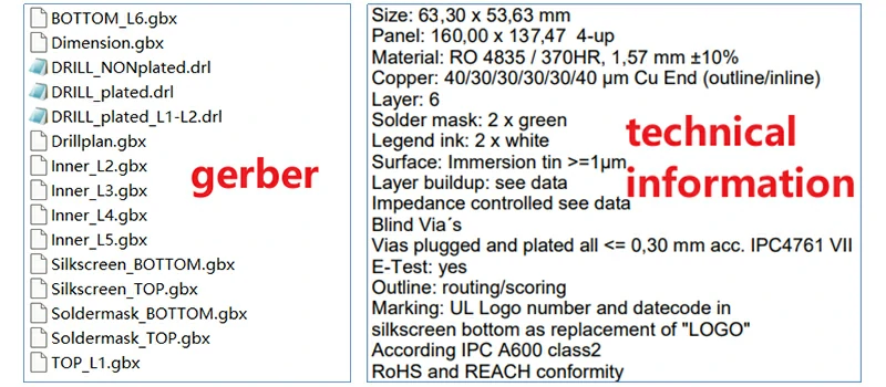
Customer data usually include gerber, and technical information such as board thickness / copper thickness / surface / solder mask color / silkscreen color / impedance / special requirement, etc.
Step 2 Check data
Factory engineer will check customer data carefully, and provide EQ (engineering query) to customer to get confirmation if have any doubt about PCB design or requirement.
Step 3 Get EQ answer
When we get EQ answer from customer,we will edit internal manufacture instruction (MI) and working gerber (used for films fabrication,such as copper layers / solder mask layers / silkscreen layers / drilling layer / outline layer,etc.)
Step 4 Start production
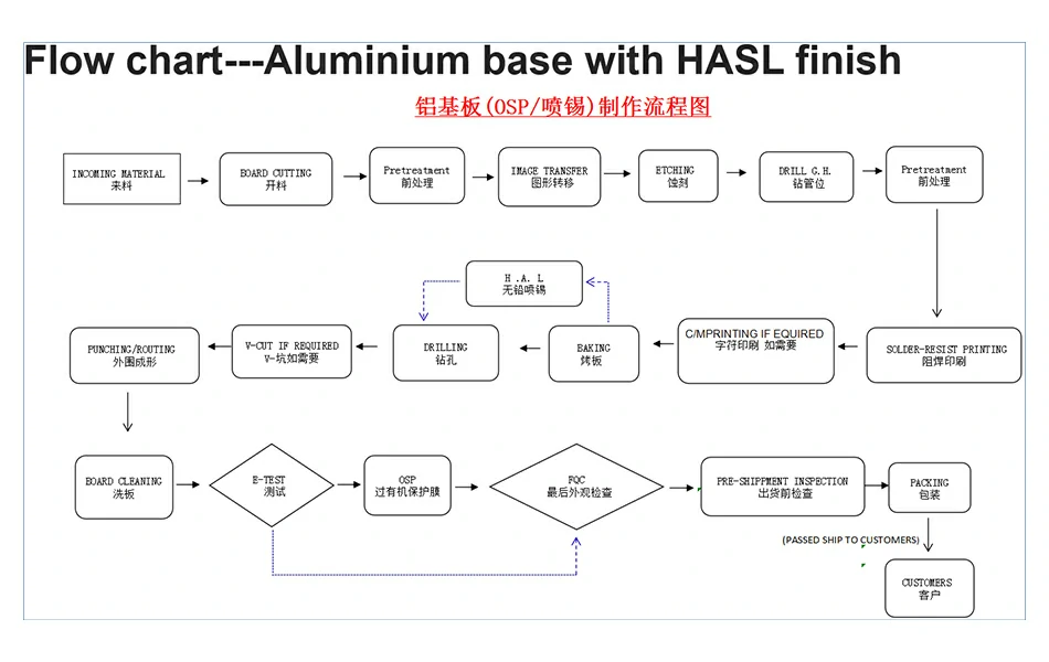
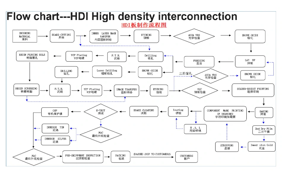
Start production, take HDI and Aluminum PCB as example, processes as follows.
Step 5 We do FAI report
We do FAI report, packing with PCBs together, and then send to customer. Shipment by different ways,such as DHL, Fedex, UPS, TNT and so on.
Start Your Project With A Free Quote
Our professionals are available to talk you through each of our offerings. We’ll be sure to answer you within 24 hours. Fill out the information below with as much detail as possible, and we’ll get back to you promptly.