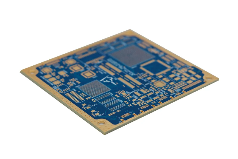
| Layers: | 6 Layers |
| Material: | FR4 TG170 |
| Finish board thickness: | 1.6mm |
| Finish copper thickness: | 1 oz |
| Surface treatment: | ENIG |
| Solder mask: | Green |
| Notes: | UL/ISO/IATF16949/SGS certification, Halogen free |
HDI (High Density Interconnect) is a high density interconnect technology that enables more tracks and interconnect through holes. Compared to traditional circuit boards, HDI technology can achieve more functions in a smaller size.
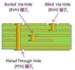
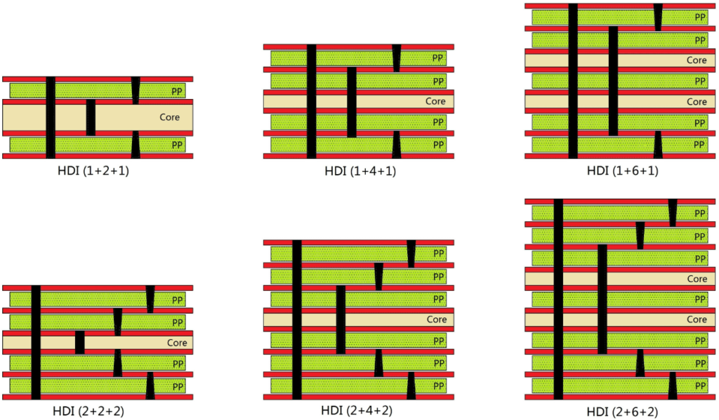
HDI technology mainly realizes high density interconnection through the following aspects: First, through the design of micro-tracks and holes, more tracks can be realized in a limited space; Secondly, using blind hole and buried hole technology, electrical connection between different layers can be realized, thus reducing the layer spacing; In addition, the stackup of micro-lines and inner layer crossing of tracks are also used to further improve the line density and interconnection performance.
1.High density: The biggest feature of HDI board is high density. Compared to traditional printed circuit board (PCB),HDI boards have a smaller line width/space, allowing for higher component density. This not only helps to reduce the volume and weight of the product, but also improves the performance and reliability of the product.
2.Small size: Due to the high-density nature of the HDI board, it can achieve a smaller size while maintaining high performance. This is especially important for high-end electronics that need to integrate more functions into a limited space, such as smartphones, tablets and wearables.
3.High-speed signal transmission: The HDI board uses a fine line design, which can achieve high-speed and stable signal transmission. This is critical for high-end electronics that need to process large amounts of data in real time, such as data centers, cloud computing, and artificial intelligence devices.
4.Strong anti-interference ability: the high-frequency characteristics of the HDI board make it have strong anti-interference ability, which can effectively reduce the impact of electromagnetic interference on product performance. This is especially important for high-end electronics that work in complex environments, such as aerospace, military, and medical devices.
5.Environmental protection and energy saving: HDI board uses environmentally friendly materials and processes, which can reduce the energy consumption and emissions of the product.
HDI technology is widely used in computer, mobile communication, medical equipment, automotive electronics, military, Internet of Things (LoT) and other fields, providing possibilities for miniaturized and high-performance electronic products.
