At Tri-Win Circuits, we transform complex digital designs into the physical backbones of modern electronics every single day. A Printed Circuit Board (PCB) might seem like a simple green board, but the journey from a design file to a fully functional, reliable circuit board is a meticulous, multi-step process blending chemistry, engineering, and precision manufacturing. Understanding this process is key to appreciating the quality and complexity behind the devices you use daily.
Let’s peel back the layers and explore the intricate journey of PCB fabrication, showing you exactly how your vision becomes a tangible, high-performance product.
Table of Contents
The Digital Blueprint: Starting with Your Design
Every great physical product begins as a digital idea. For PCBs, this idea is encapsulated in a set of design files, most commonly the Gerber files. These files act as the master blueprint, providing a layer-by-layer instruction manual for our manufacturing equipment. Each file corresponds to a specific layer of the PCB: the copper traces, solder mask, silkscreen, drill locations, and board outline.
Before we even think about cutting materials, the first and most critical quality check happens here. Our engineers at Tri-Win Circuits perform a thorough Design for Manufacturability (DFM) check. This analysis scrutinizes your design against our production capabilities to identify potential issues that could affect yield, performance, or cost. We look for things like trace widths that are too thin, insufficient clearance between elements, and missing drill data. Proactively catching these issues saves you time and money, ensuring a smooth production run from the very start.
How Are Circuit Boards Actually Made? The Core Fabrication Steps
Once your design is verified, the physical creation begins. The process varies slightly between single-sided, double-sided, and multi-layer boards, but the core principles remain the same. We are essentially building the board from the inside out.
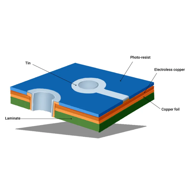
For a multi-layer PCB, the process starts with the inner layers. We take a core laminate material (often FR-4) clad with copper foil. A light-sensitive film called a photoresist is applied. We then expose this film to UV light through a photomask of your design, hardening the resist over the areas that will become copper traces. The unhardened resist is washed away, and the board is submerged in an etching solution that removes the exposed copper. What remains is the perfect copper circuitry of your inner layers, protected by the hardened photoresist, which is then stripped away.
Next, the layers are stacked. For multi-layer boards, the etched inner-layer cores are stacked with layers of “prepreg”—a fiberglass cloth pre-impregnated with epoxy resin. This entire stack-up, including outer layers of copper foil, is then placed in a massive lamination press. Under immense pressure and high temperature, the prepreg resin melts and fuses the layers together into a single, solid multi-layer board.
With the layers fused, it’s time to create the electrical pathways between them. A high-speed, computer-controlled drill creates all the necessary holes, known as vias, as well as mounting holes and component leads. Precision here is paramount; even a minuscule deviation can ruin the board. After drilling, the board goes through a chemical process of electroless copper deposition, which coats a micro-thin layer of copper on the entire surface, including the inside walls of the newly drilled holes. This is followed by electrolytic plating, which adds a thicker, more robust layer of copper, creating the conductive channels known as Plated Through-Holes (PTH).
The process of imaging and etching is then repeated for the outer layers, defining the final circuit patterns you see on the outside of the board.
What Are the Crucial Layers Applied to a Bare Board?
With the copper circuitry established, we must add protective and informative layers to prepare the board for assembly.
First is the Solder Mask. This is the typically green (though other colors are available) layer that covers the entire board except for the pads where components will be soldered. Its purpose is twofold: it protects the copper traces from oxidation and damage, and it prevents “solder bridges”—accidental shorts that can occur between closely spaced pads during the assembly process. The solder mask is applied as a liquid and then cured with UV light for a hard, durable finish.
Next comes the Silkscreen, also known as the legend. This is the white (or other colored) ink layer that prints reference designators, component outlines, logos, and other helpful information directly onto the board. A clear and accurate silkscreen is vital for efficient hand-soldering, automated assembly, and future debugging or repair work.
How Do We Ensure PCB Quality and Durability?
The exposed copper pads where components will be attached need protection from the elements to ensure good solderability. This is achieved by applying a Surface Finish. The choice of finish depends on the application, cost, and components being used. Each has its own set of advantages.
| Surface Finish Type | Description | Advantages | Considerations |
|---|---|---|---|
| HASL (Hot Air Solder Leveling) | The board is dipped in molten solder and then leveled with hot air knives. | Low cost, excellent solderability, widely available. | Not perfectly flat, not ideal for fine-pitch components. Lead-free versions available. |
| ENIG (Electroless Nickel Immersion Gold) | A layer of nickel is chemically deposited, followed by a thin layer of immersion gold. | Very flat surface, excellent for fine-pitch and BGA components, good shelf life. | Higher cost, more complex process. |
| OSP (Organic Solderability Preservative) | A thin, organic layer is applied to the copper to protect it before soldering. | Flat surface, environmentally friendly, low cost. | Shorter shelf life, can be sensitive to handling. |
After the surface finish is applied, the boards undergo rigorous testing. Every multi-layer board we produce at Tri-Win Circuits is subjected to an Electrical Test (E-Test). A flying probe or bed-of-nails tester checks every net on the board to ensure continuity (no open circuits) and isolation (no short circuits). This guarantees the board is electrically perfect according to your design file. We also use Automated Optical Inspection (AOI) at various stages to visually scan for manufacturing defects.
Finally, the individual boards are separated from the larger manufacturing panel through routing or v-scoring. A final visual inspection is performed, and the boards are vacuum-sealed and packaged, ready for shipment or for our in-house PCBA assembly line.
Why Does Your Choice of PCB Manufacturer Matter?
As you can see, the PCB fabrication process is a symphony of precise, interconnected steps. A failure at any stage can compromise the integrity of the final product. The difference between a functional prototype and a reliable, mass-produced product often comes down to the expertise, technology, and quality control of the manufacturer.
At Tri-Win Circuits, we don’t just fabricate boards; we build partnerships. We combine state-of-the-art technology with a relentless commitment to quality and customer service. Our DFM checks, in-process inspections, and comprehensive final testing are all designed to give you peace of mind and ensure your product performs exactly as intended.
Whether you need a quick-turn prototype or high-volume production, our team is ready to bring your design to life with the quality and reliability you deserve. Contact us today to discuss your next project and experience the Tri-Win Circuits difference.


