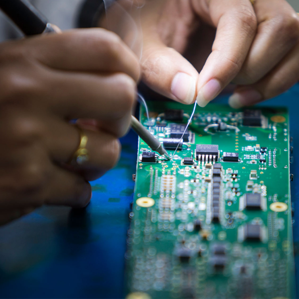
In high-speed digital and RF circuits, signal integrity is everything. A design that looks perfect in simulation can fail in the real world due to impedance mismatches, leading to costly delays, board respins, and performance issues. The critical link between your design intent and a successfully manufactured PCB is a set of clear, precise, and complete fabrication notes.
At Tri-Win Circuits, we’ve seen firsthand how ambiguous notes can create production challenges. We’ve also seen how a little extra detail can ensure a project is a first-pass success. Tri-Win Circuits is written from our perspective as your fabrication partner. We want to demystify the process and give you the exact tools you need to write fabrication notes that guarantee your impedance requirements are met, every single time.
What is Controlled Impedance and Why It Matters
In simple terms, controlled impedance is the management of the characteristic impedance of a PCB trace to a specific value. For high-frequency signals (like those in USB, HDMI, DDR memory, and antenna feeds), the trace acts as a transmission line. If the trace’s impedance doesn’t match the source and load impedance, signal reflections occur. These reflections corrupt your data, causing errors, jitter, and a complete failure of the device.
By controlling the impedance, we ensure a smooth, uninterrupted flow of energy and data. This is achieved by carefully controlling three physical factors during manufacturing:
- The width and thickness of the copper trace.
- The thickness of the dielectric material (core or prepreg) between the trace and its reference plane.
- The dielectric constant (Er) of that material.
The Essential Checklist: 5 Must-Haves for Your Controlled Impedance Fab Notes
To ensure we build your board exactly as you designed it, your fabrication notes must be unambiguous. Vague instructions like “Control impedance on high-speed lines” are not actionable. Use this checklist to provide all the necessary information.
1. Clearly Identify Target Traces
We need to know exactly which traces require impedance control. You can do this in two primary ways, and we recommend using both for maximum clarity.
- By Net Name: List the specific net names or use wildcards. This is the most precise method. Example: “Control impedance for all nets named USB_D_P, USB_D_N, and TX_*”
- By Graphical Callout: On a separate fabrication drawing layer, graphically highlight the controlled traces. This provides excellent visual confirmation.
2. Specify Impedance Value and Type
State the target impedance value in ohms and specify the trace configuration. There are two main types:
- Single-Ended: A single trace referenced to a plane. Example: “50-ohm single-ended.”
- Differential Pair: Two coupled traces that carry differential signals. Example: “100-ohm differential.”
Be explicit. A note for “100 ohms” is unclear—is that a single-ended trace or a differential pair?
3. Define the Tolerance
How close do we need to be to the target value? The industry standard is +/- 10%, which is suitable for most digital applications. For more sensitive RF or precision applications, you might require a tighter tolerance like +/- 7% or +/- 5%. Be aware that requesting tighter tolerances can impact manufacturing yield and cost, so only specify it when truly necessary.
4. Reference the Exact Layer Stack-up
Your impedance notes must correspond directly to your layer stack-up. The note should specify which layer the controlled trace resides on. This confirms that the trace width and dielectric spacing calculated in your design match the layer we will be manufacturing.
Example: “50-ohm traces on Layer 1 (Top) and Layer 8 (Bottom).”
5. Detail the Reference Planes
A trace’s impedance is defined relative to its reference plane(s). Your note must specify which plane(s) the signal is referenced to. This is especially critical in multi-layer boards.
Example: “Referenced to the GND plane on Layer 2” or “Referenced between the PWR plane on Layer 4 and the GND plane on Layer 6.”
A Practical Example: A Perfect Fabrication Note
Here is what an ideal, consolidated set of controlled impedance notes looks like in a fabrication drawing. It is clear, concise, and contains all five essential elements.
CONTROLLED IMPEDANCE NOTES:

1. 100 OHM DIFFERENTIAL (+/- 10%) ON NETS U1_TX_P/N & U2_RX_P/N. TRACES ARE ON LAYER 3 (SIG1) AND REFERENCED TO GND PLANE ON LAYER 4.

2. 50 OHM SINGLE-ENDED (+/- 10%) ON NET RF_ANT. TRACE IS ON LAYER 1 (TOP) AND REFERENCED TO GND PLANE ON LAYER 2.

3. FABRICATOR TO ADJUST TRACE WIDTHS AS NEEDED TO MEET IMPEDANCE TARGETS. FINAL STACK-UP REQUIRES CUSTOMER APPROVAL.

4. INCLUDE IMPEDANCE TEST COUPONS FOR ALL CONTROLLED LINES ON PRODUCTION PANEL. TDR TEST REPORT REQUIRED WITH SHIPMENT.
Beyond the Notes: How Collaboration Ensures Success
Excellent notes are the starting point, but a truly successful outcome relies on a partnership between you and your fabricator. At Tri-Win Circuits, we see ourselves as an extension of your engineering team.
Your Stack-up: The Foundation of Success
The layer stack-up is the blueprint for impedance. While you should provide a proposed stack-up with your design files, allow for flexibility. Our engineers use advanced modeling software to analyze your impedance requirements. We may suggest minor adjustments to trace widths or dielectric materials to optimize for manufacturability, reliability, and cost—all while guaranteeing we hit your target impedance. This collaborative approach prevents issues before they ever reach the production floor.
Test Coupons: Your Manufacturing Insurance Policy
How do you know the impedance was met? We add test coupons to the production panel alongside your boards. These coupons replicate your controlled trace geometries. After fabrication, we use a Time Domain Reflectometer (TDR) to measure the impedance of these coupons. This provides an objective, data-backed report confirming that the manufactured boards meet your specified tolerance.
Early Communication is Key
Don’t wait until the design is finalized to think about fabrication. The best time to engage with us is during the layout phase. By discussing your stack-up and impedance needs early, we can provide feedback that saves you from a potential redesign. A quick conversation can confirm material availability and process capabilities, ensuring a smooth and predictable manufacturing run.
Why Partner with Tri-Win Circuits for Your Controlled Impedance PCBs?
Successfully manufacturing controlled impedance PCBs requires more than just equipment; it requires expertise, precise process control, and a commitment to quality. At Tri-Win Circuits, this is one of our core strengths.
- Experienced Engineers: Our team reviews every high-speed design, providing feedback to optimize for performance and manufacturability.
- Advanced Process Control: We tightly control every variable, from etching to lamination, to ensure your impedance targets are met with precision.
- In-House TDR Testing: We don’t guess. We verify every controlled impedance job with TDR testing and provide you with a comprehensive report for your records.
- Collaborative Partnership: We believe in working with you. From stack-up design to final testing, we are your partners in creating a successful, high-performance product.
Clear fabrication notes are the foundation of a successful high-speed PCB. By following this guide, you can eliminate ambiguity and ensure your design intent is perfectly translated into a physical product.
Ready to ensure your next high-speed design is a first-pass success? Upload your design files to Tri-Win Circuits today, and let our experts help you get it right the first time.


