At the heart of every electronic device lies a Printed Circuit Board (PCB), the silent, foundational hero of modern technology. And on that board, an intricate network of pathways forms the central nervous system that allows components to communicate. These pathways are known as PCB traces. As a leading one-stop solution for PCB fabrication and assembly, Tri-Win Circuits understands that the quality of these traces is paramount to the performance and reliability of your final product.
This comprehensive guide will explore what PCB traces are, the critical design parameters to consider, and how our meticulous fabrication process brings them to life.
- What is a PCB Trace? The Veins of Your Circuit
- Key Characteristics of a PCB Trace
- The Critical Role of Traces in PCB Design
- The PCB Trace Fabrication Process: From Design to Reality
- Why Your Fabrication Partner is Crucial for Perfect Traces
- Conclusion: Partner with Tri-Win Circuits for Flawless PCB Fabrication
What is a PCB Trace? The Veins of Your Circuit
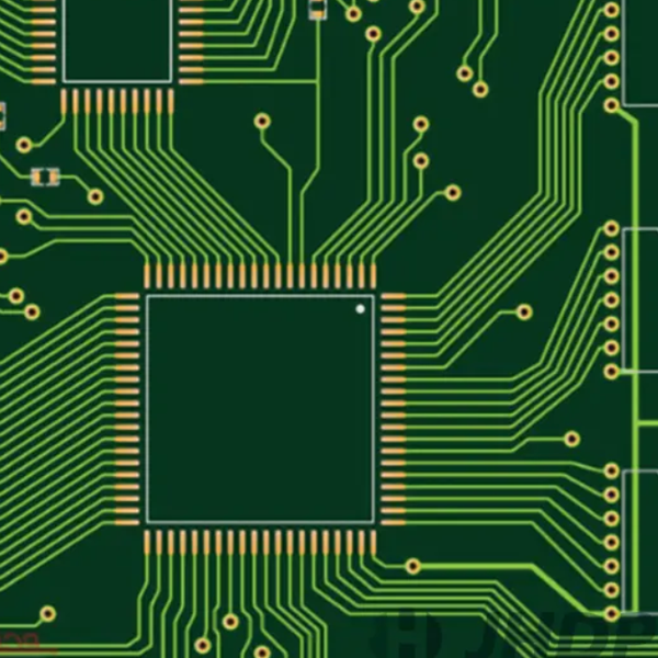
A PCB trace is a flat, narrow conductive path, typically made of copper, that is etched onto a non-conductive substrate material of a printed circuit board. Think of traces as the wires of your circuit, but instead of being separate components, they are integrated directly into the board’s structure.
Their primary functions are to:
- Carry Signals: Transmit data and control signals between different components, like a microprocessor and memory.
- Distribute Power: Deliver the necessary voltage and current from the power source to all active components on the board.
- Provide Grounding: Establish a common reference point (ground) for the circuit, which is essential for stability and signal integrity.
The precision, integrity, and quality of these traces directly impact the overall functionality and lifespan of the electronic device.
Key Characteristics of a PCB Trace
Designing and fabricating a reliable PCB requires a deep understanding of the fundamental properties of traces. At Tri-Win Circuits, our engineers pay close attention to these three key characteristics during our Design for Manufacturability (DFM) review.
Trace Width
The width of a trace is a critical parameter that determines its current-carrying capacity. A wider trace has a lower electrical resistance and can safely handle more current without overheating. Power lines and ground planes typically require much wider traces than low-power digital signal lines. Failing to properly size trace width can lead to overheating, voltage drops, or even a burnt-out, failed board.
Trace Thickness (Copper Weight)
Trace thickness is defined by the weight of the copper foil used on the substrate, measured in ounces per square foot (oz/ft²). Common values are 1 oz (standard) and 2 oz (heavy copper). Like width, thickness also affects current capacity and heat dissipation. Thicker copper allows for a higher current to be passed through a trace of the same width, making it crucial for high-power applications.
Trace Spacing (Clearance)
Spacing refers to the minimum air gap maintained between adjacent traces or between a trace and a pad. This clearance is vital for preventing electrical issues such as arcing (an electrical discharge between conductors) at high voltages and crosstalk (unwanted signal interference) in high-frequency circuits. The required spacing depends on the voltage, impedance requirements, and the manufacturing capabilities of your fabrication partner.
The Critical Role of Traces in PCB Design
A well-thought-out trace layout is the difference between a high-performance circuit and a problematic one. Effective design goes beyond simply connecting points A and B.
Ensuring Signal Integrity
For high-speed digital circuits (e.g., in Rogers or HDI PCBs), maintaining signal integrity is key. This involves techniques like impedance control, where the trace width and its distance from a ground plane are precisely controlled to maintain a specific impedance (e.g., 50 ohms). This prevents signal reflections and ensures data is transmitted cleanly.
Managing Current and Heat
As mentioned, traces carrying significant current must be wide enough to prevent overheating. In addition to proper width, designers may use large copper pours (planes) connected to high-current traces to act as heatsinks, effectively dissipating thermal energy and improving the reliability of components.
Routing Strategies
Best practices in trace routing include avoiding sharp 90-degree angles (which can cause signal reflections) in favor of 45-degree bends or curved paths. For sensitive differential signals, traces are routed as a pair with consistent spacing to minimize noise interference.
The PCB Trace Fabrication Process: From Design to Reality
So, how are these intricate networks created? This is where a professional fabrication partner like Tri-Win Circuits comes in. We transform your digital design file into a physical, high-quality PCB through a precise, multi-step process.
- Design File Review: Our process begins with a thorough DFM check of your Gerber or CAD files. Our experienced engineers look for potential issues with trace width, spacing, and other parameters that could affect manufacturability or performance.
- Imaging (Photolithography): A sheet of copper-clad laminate (the base material, like FR-4) is cleaned and coated with a light-sensitive film called photoresist. Your circuit design is printed onto a photomask, which is then placed over the board and exposed to high-intensity UV light. The light hardens the photoresist in the areas that will become your traces.
- Etching: The board is submerged in a chemical solution (the etchant) that dissolves the unprotected copper. The hardened photoresist shields the copper underneath it, so only the unwanted copper is removed. This step leaves behind the precise network of copper traces as defined by your design.
- Stripping: After etching, the hardened photoresist that protected the traces is chemically removed, revealing the finished copper circuit pattern.
- Automated Optical Inspection (AOI): To guarantee quality, the board is scanned by our advanced AOI machines. These systems compare the fabricated board against your original design data, flagging any potential defects like short circuits (traces touching), open circuits (broken traces), or incorrect trace widths with incredible accuracy.
Why Your Fabrication Partner is Crucial for Perfect Traces
The success of your PCB hinges on the capabilities of your fabrication house. Minor deviations in the etching process, such as under-etching (not removing enough copper) or over-etching (removing too much), can lead to catastrophic failures. Choosing the right partner mitigates these risks.
Precision and Technology
At Tri-Win Circuits, we invest in state-of-the-art equipment that allows us to achieve extremely fine line widths and spacings, enabling complex and dense designs like those found in HDI boards. Our controlled processes ensure that the traces we produce match your design specifications with exacting precision.
Quality Control
Our commitment to quality is unwavering. Through rigorous steps like AOI and electrical testing, we verify the integrity of every trace on every board. This adherence to strict quality standards, backed by our UL and ISO 9001 certifications, ensures you receive a reliable and functional product.
Experience and Expertise
With over 10 years of experience, our team has the expertise to foresee potential manufacturing challenges during the DFM stage. This proactive approach saves you time and money by preventing costly redesigns and ensuring your board is optimized for robust performance.
Conclusion: Partner with Tri-Win Circuits for Flawless PCB Fabrication
PCB traces are more than just lines on a board; they are the fundamental conduits of function in every electronic device. Understanding their design principles and the precision required in their fabrication is essential for creating high-quality electronics.
By partnering with an experienced and technologically advanced manufacturer like Tri-Win Circuits, you ensure that every trace on your board is fabricated to the highest standard of quality and reliability. We are your one-stop solution, from expert DFM review to final assembly, dedicated to bringing your vision to life with unparalleled precision.
Ready to turn your complex designs into high-quality PCBs with perfectly fabricated traces? Contact the experts at Tri-Win Circuits today for a quote and experience the difference our quality and service can make.


