At Tri-Win Circuits, we live and breathe electronics. We understand the immense satisfaction that comes from creating a circuit that solves a problem, innovates a process, or simply brings a creative idea to life. For electronics enthusiasts, students, and engineers working on initial concepts, fabricating your own Printed Circuit Board (PCB) at home can be a profoundly rewarding and educational experience. It’s where the digital design meets the physical world.
Tri-Win is crafted from our professional perspective to walk you through the process of homemade PCB fabrication. We’ll cover the popular methods, essential safety precautions, and help you understand when your project is ready to graduate from a DIY board to a professionally manufactured one.
Before You Begin: Is DIY PCB Making Right for You?
Making a PCB at home is an excellent skill. However, it’s important to weigh the pros and cons before you start investing in equipment and materials.
Advantages of DIY PCBs:
- Learning Experience: It provides invaluable insight into the fundamentals of PCB structure and manufacturing.
- Speed for Simple Prototypes: For a very simple, single-sided board, you can potentially go from design to a physical board in a few hours.
- Cost-Effective for One-Offs: If you only need one or two simple boards, the material cost can be lower than a minimum order from a professional fab house.
Challenges of DIY PCBs:
- Limited Complexity: DIY methods are generally restricted to single or double-sided boards. Plated through-holes (vias), multi-layer boards, and controlled impedance are nearly impossible to achieve at home.
- Safety Risks: The process involves hazardous chemicals (like etchants) that require careful handling, ventilation, and proper disposal.
- Lower Precision: Achieving very fine traces and clearances is difficult, limiting you from using modern surface-mount (SMD) components with a fine pitch.
- No Solder Mask or Silkscreen: These professional layers, which prevent solder bridges and identify components, are typically absent on DIY boards, making assembly more difficult and the board less durable.
Essential Tools and Materials You’ll Need
While specific items depend on the method, here is a general list of what you’ll need to get started:
- Copper Clad Board: A basic FR-4 board with a thin layer of copper. Single-sided is best for beginners.
- PCB Design Software: KiCad, Eagle, or EasyEDA are popular choices for creating your layout.
- Printing: A laser printer (for Toner Transfer) or an inkjet printer with transparencies (for Photoresist).
- Etchant: Ferric Chloride or Sodium Persulfate are common choices. (Handle with extreme care!)
- Safety Gear: Nitrile gloves, safety goggles, and a well-ventilated workspace are non-negotiable.
- Tools for Cutting & Cleaning: A small saw or shear for cutting the board, and steel wool or a scouring pad for cleaning the copper.
- Drilling: A Dremel or a small PCB drill press with fine drill bits.
- Household Iron or Laminator: For the Toner Transfer method.
- UV Light Source: For the Photoresist method.
Step 1: Designing Your Circuit for DIY Fabrication
Before you touch any hardware, your design must be ready. When designing for a homemade PCB, you need to be less ambitious than you would be for a professional board.
- Use Thicker Traces: Aim for trace widths of 20 mil (0.5mm) or greater. This makes them more resilient to imperfections in the etching process.
- Increase Clearances: Keep ample space between traces and pads to prevent accidental shorts.
- Choose Larger Component Footprints: Through-hole components or larger SMD packages (like 1206 or 0805) are much easier to work with than fine-pitch parts.
- Print a Mirror Image: When you print your design, you must print a mirrored version. When you transfer it to the copper side of the board, it will then be in the correct orientation.
Step 2: Choosing Your Home Fabrication Method
Two methods dominate the DIY PCB scene. Let’s explore them.
Method A: The Toner Transfer (Iron-On) Method
This is the most common and accessible method for beginners. It uses the toner from a laser printer as an “etch resist.”
- Print Your Design: Print the mirrored layout onto glossy magazine paper or special toner transfer paper using a laser printer at the highest quality setting.
- Prepare the Board: Cut your copper-clad board to size. Thoroughly clean the copper surface with steel wool or a scouring pad until it is shiny, then wipe it clean with isopropyl alcohol to remove any oils.
- Transfer the Toner: Place the printed design toner-side-down onto the clean copper. Using a household iron on its highest setting (no steam), apply firm, even pressure for several minutes. The heat melts the toner, fusing it to the copper. A laminator can also provide more even heat and pressure.
- Remove the Paper: Submerge the hot board in warm water for about 10 minutes. The paper will soften, and you can gently peel and rub it away, leaving just the black toner traces on the copper.
Pros: Cheap, fast, and requires no special lighting equipment.
Cons: Can be inconsistent; achieving 100% toner transfer without breaks in traces can be tricky.
Method B: The UV Photoresist Method
This method is more complex but yields much finer and more professional-looking results.
- Print Your Design: Print your mirrored layout onto a transparent acetate sheet. You need a high-contrast, opaque print.
- Apply the Film: In a dimly lit room, apply the photosensitive film (dry film) to your clean copper board, squeegeeing out any air bubbles.
- Expose to UV Light: Place your transparency on top of the film-covered board and expose it to a UV light source. The UV light hardens the film in the areas not covered by your black traces. The areas corresponding to your traces remain soft.
- Develop the Image: Submerge the board in a developer solution (often a weak sodium carbonate solution). The unexposed, soft film will wash away, revealing the copper underneath your trace pattern. The hardened film remains as the etch resist.
Pros: Capable of much finer lines and greater detail. More reliable than toner transfer.
Cons: Requires more specific materials (film, developer, UV light) and is more sensitive to process variables.
Step 3: The Critical Etching Process & Safety
This is the stage where the unwanted copper is chemically removed, leaving only your circuit traces. It is also the most dangerous step.
SAFETY WARNING
Etchants like Ferric Chloride are corrosive and toxic. Always work in a well-ventilated area (preferably outdoors), wear safety goggles and chemical-resistant gloves. Never pour used etchant down the drain. It must be neutralized and taken to a hazardous waste disposal facility.
- Prepare the Etchant Bath: Gently heat the etchant in a plastic container. A warm etchant works much faster.
- Submerge the Board: Place your board in the etchant. Agitate the container continuously to ensure fresh etchant is always in contact with the copper.
- Monitor Progress: The exposed copper will slowly dissolve. The process can take anywhere from 10 to 30 minutes. Once all the unwanted copper is gone, remove the board using plastic tongs.
- Neutralize and Clean: Rinse the board thoroughly in a neutralizing bath (like a baking soda and water solution) and then with plain water. Finally, use acetone or alcohol to scrub off the remaining toner or photoresist, revealing your shiny copper traces.
Step 4: Drilling, Cleaning, and Finishing Touches
Your board is etched, but it’s not ready yet.
- Drilling: Using a drill press or Dremel, carefully drill the holes for your through-hole components. Use a sharp, correctly sized bit to avoid damaging the pads.
- Tinning (Optional): To protect the copper from oxidation and make soldering easier, you can “tin” the board using chemical tinning solutions or by applying a thin coat of solder with an iron and solder wick.
When to Go Pro: The Limits of DIY and The Power of Professional Manufacturing
Congratulations! You’ve made a PCB. For many hobby projects, this is all you need. However, as your designs become more sophisticated, you will quickly encounter the limitations of homemade boards. This is the point where a professional PCB manufacturer becomes your most valuable partner.
Consider a professional service like Tri-Win Circuits when your project requires:
- Multi-Layer Boards: Any design with more than two layers requires professional fabrication.
- Plated Through-Holes (Vias): Essential for connecting traces between layers, vias must be electroplated for reliability—a process that can’t be done at home.
- Fine Pitch Components: To use modern, high-performance ICs, you need the high precision and tight tolerances that only professional manufacturing can guarantee.
- Solder Mask and Silkscreen: A professional board includes a solder mask to prevent shorts during assembly and a silkscreen to label components, dramatically improving assembly speed and reducing errors.
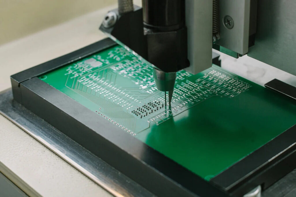
- Guaranteed Quality and Reliability: Professional fabs use automated optical inspection (AOI) and electrical testing to ensure every connection is perfect. This is crucial for products that need to be dependable.
- Volume Production: When you need more than just a few boards, professional manufacturing is infinitely more time and cost-effective.
Tri-Win Circuits: Your Partner for Flawless PCBs
We celebrate the spirit of DIY innovation because that’s where great ideas are born. When your great idea is ready for the next level, Tri-Win Circuits is here to help you realize its full potential.
We offer quick-turn prototyping that delivers professional-grade, multi-layer PCBs to your door, often faster than you could reliably make one yourself. From rigid FR-4 and advanced materials to flexible and rigid-flex circuits, our state-of-the-art facility can handle any level of complexity. Paired with our PCB assembly services, we provide a true one-stop solution to take your design from a file to a fully functional, production-quality device.
Keep experimenting, keep learning, and when you’re ready to build something robust, reliable, and truly professional, get in touch with us. We’re here to help you win.


