In the fast-paced world of electronics, efficiency and cost-effectiveness are paramount. While individual Printed Circuit Boards (PCBs) are the building blocks of virtually all electronic devices, manufacturing them one by one can be a slow and expensive process. This is where PCB panelization comes in—a critical technique that revolutionizes how PCBs are made, ensuring faster production, lower costs, and higher quality.
This article will serve as your ultimate guide to PCB panelization, detailing what it is, its undeniable benefits, the various methods employed, crucial design considerations, and how it all culminates in the final product.
I. Introduction: The Foundation of Modern PCB Manufacturing
The journey of an electronic device begins with its PCB. From tiny wearables to complex industrial machinery, every board must be precisely fabricated and assembled. However, handling and processing thousands of tiny, individual PCBs through an automated assembly line presents significant challenges regarding speed, manual labor, and material waste.
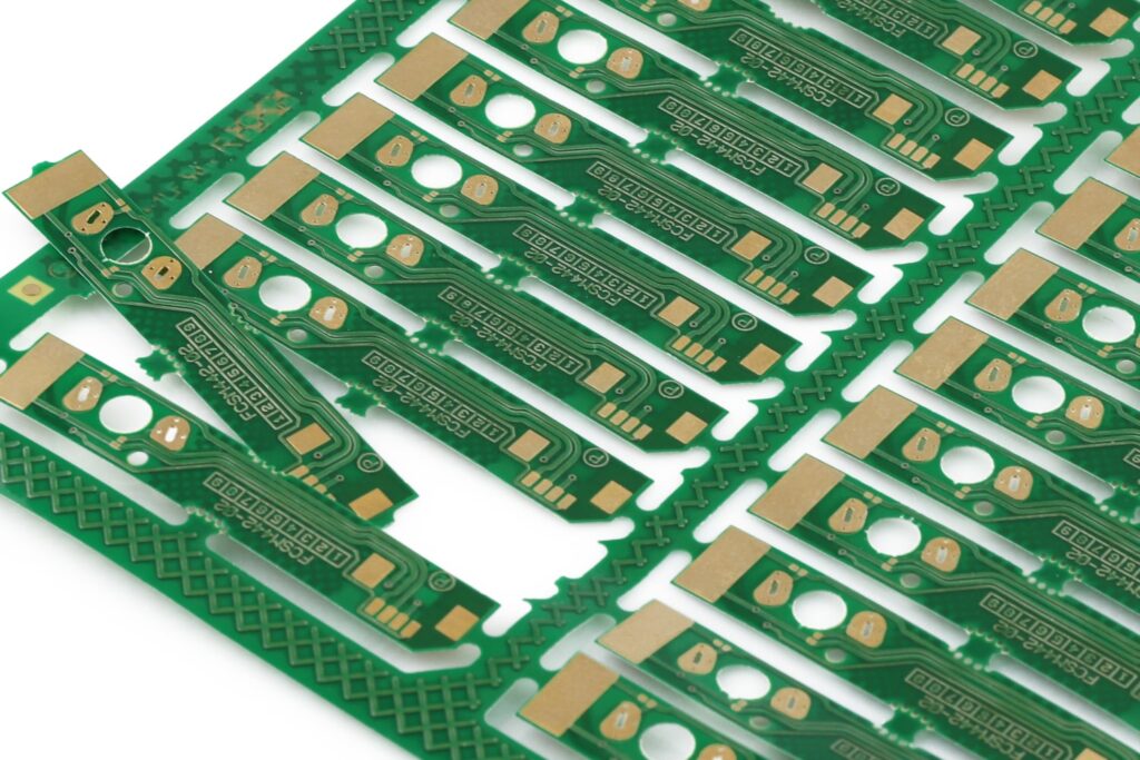
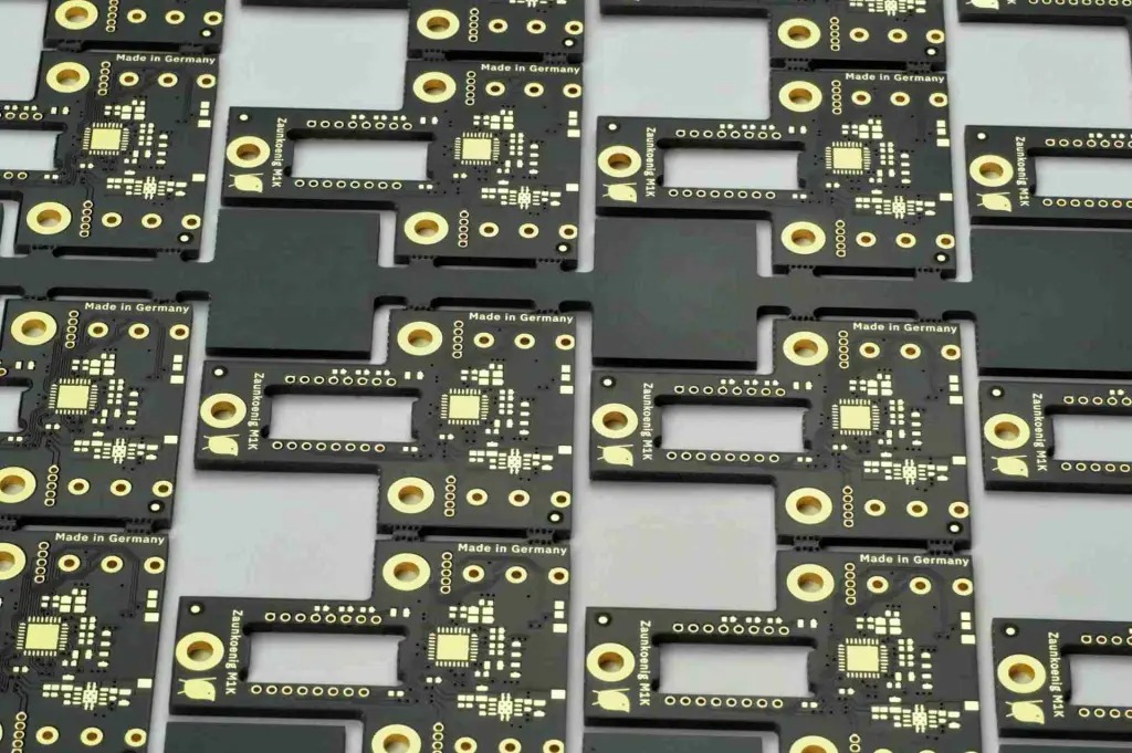
PCB panelization, also known as array creation, is the ingenious solution to this problem. It involves combining multiple individual Printed Circuit Boards (PCBs) onto a larger, single manufacturing panel, or array. Think of it as creating a “sheet” of PCBs that can be processed as one unit. This single panel then moves through various stages of manufacturing, including solder paste application, component placement, soldering, and inspection, dramatically streamlining the entire production flow. The core purpose is simple: to optimize manufacturing for peak efficiency, significant cost reductions, and superior quality control.
II. Why Panelize? The Indisputable Benefits of PCB Arrays
The adoption of PCB panelization is driven by its compelling advantages across the entire production cycle:
A. Cost Reduction
Panelization plays a significant role in lowering manufacturing costs:
- Material Efficiency: It maximizes the utilization of raw PCB laminate. By arranging multiple boards on a standard sheet, waste from individual board cutouts is significantly minimized, leading to substantial material cost savings.
- Labor Savings: Automated assembly lines can process one large panel far more efficiently than numerous individual boards. This reduces manual handling, setup times, and the associated labor costs.
- Economies of Scale: Processing boards in batches through panels allows manufacturers to achieve economies of scale in material procurement and machine operation, further driving down the per-board cost.
B. Enhanced Manufacturing Efficiency & Speed
Speed and efficiency are dramatically improved with panelization:
- Automated Assembly Optimization: Automated machines like pick-and-place robots, reflow ovens, and stencil printers are designed to handle larger panels. Panelization dramatically speeds up component placement, soldering, and other processes by allowing multiple boards to be worked on simultaneously.
- Increased Throughput: With multiple PCBs being processed as a single unit, the overall output rate (throughput) of the manufacturing line is significantly boosted.
- Smoother Workflow: The standardized size and structure of a panel lead to a more consistent and predictable flow through the assembly line, reducing bottlenecks and improving overall production planning.
C. Improved Quality Control & Reliability
Panelization contributes to higher product quality:
- Consistent Processing: Every individual board on a panel undergoes identical processing conditions. This uniformity contributes to higher, more consistent quality across all manufactured PCBs.
- Easier Inspection: Automated Optical Inspection (AOI) systems and electrical test fixtures can inspect and test the entire panel more quickly and accurately than individual boards, catching defects earlier in the process.
- Component Protection: The structural integrity of the panel provides a degree of protection to individual PCBs and their delicate components from physical stress or damage during handling and transportation between manufacturing stages.
D. Enabling Production of Small & Irregular Boards
Many automated assembly machines have minimum size requirements for PCBs they can handle. Panelization allows for the manufacturing of very small or unusually shaped boards that would otherwise be impossible or highly impractical to produce individually.
III. Key PCB Panelization Methods: Choosing the Right Strategy
The method of panelization largely depends on the PCB’s design, shape, and specific manufacturing requirements. The two most common methods are V-scoring and Tab Routing.
A. V-Scoring (V-Groove Panelization)
- Description: This method involves cutting V-shaped grooves along the top and bottom surfaces of the panel using a specialized blade. These cuts partially separate the boards, leaving a thin “web” of material that holds them together.
- Ideal Use Cases: V-scoring is best suited for rectangular or square PCBs with straight edges, where high-volume, rapid depanelization is critical.
- Advantages: It is highly cost-effective, requires minimal space between individual boards (allowing more boards per panel), and allows for very fast separation.
- Disadvantages: Creates stress lines along the score, meaning components, especially sensitive ones, must be kept a safe distance from the V-grooves. It is unsuitable for boards with non-straight edges or complex shapes.
B. Tab Routing (Breakaway Tabs with Mouse Bites)
- Description: With this method, a router bit cuts the outline of each individual PCB from the panel, leaving small connecting “tabs” or bridges of material at specific points to hold the boards in the array. To facilitate easier and cleaner separation, small, perforated holes—known as “mouse bites”—are often added within these tabs.
- Ideal Use Cases: Tab routing is highly versatile and is the go-to method for irregularly shaped PCBs, boards with overhanging components, or those requiring very smooth, clean edges after separation.
- Advantages: Offers high design flexibility for various board shapes, effectively protects components near edges, and results in cleaner edges post-depanelization (especially with well-designed mouse bites).
- Disadvantages: Requires more space between individual boards (to accommodate the router bit’s path), can be slightly more expensive per panel, and depanelization is generally slower than V-scoring.
C. Advanced & Specialized Methods (Brief Mentions)
- Laser Cutting: This high-precision method uses a laser to cut the individual boards from the panel. It offers exceptional accuracy and creates virtually no mechanical stress on the board, making it ideal for highly intricate designs or very delicate components. However, it is generally slower and more expensive.
- Punch and Die: For very high-volume, specific applications, a custom punch and die tool can be used to quickly separate boards.
IV. Essential Design Considerations for Effective PCB Panelization (Design for Manufacturability – DFM)
Successful PCB panelization begins long before manufacturing—it starts in the design phase. Adhering to Design for Manufacturability (DFM) guidelines is crucial to avoid issues during assembly and depanelization.
A. Panel Dimensions & Layout Optimization
Work closely with your fabricator (like TriWin PCB) to understand their standard panel sizes. Optimize the arrangement of your individual boards on the panel to maximize the number of boards per array, thereby maximizing material utilization and reducing costs. This often involves carefully considering board shape and rotation.
B. Board-to-Board Spacing & Edge Clearance
Ensure there’s sufficient spacing between individual PCBs on the panel. This minimum distance is critical for the chosen panelization method (e.g., clearance for the V-score blade or the router bit’s width). Also, guarantee adequate clearance between components on the PCB and the panel’s edges, score lines, or tabs.
C. Critical Component Placement (DFM for Thermal Management)
This is a crucial design point. Sensitive or tall components, especially those that extend near the board’s edge, must be strategically placed away from V-grooves or breakaway tabs. This prevents mechanical stress and potential damage during the depanelization process.
While optimizing for panelization streamlines manufacturing, the functionality of the individual PCB remains paramount. This includes rigorous thermal management design. For high-power applications, components like MOSFETs often generate significant heat, requiring robust heatsinks to ensure reliable operation. When designing your PCB panel, it’s crucial to ensure that the placement of such thermally sensitive components, and the space allocated for their fet heatsinks, does not interfere with the chosen panelization method or the subsequent depanelization process. Careful consideration at the design stage prevents potential damage to heatsinks or the components they cool when separating boards from the panel.
D. Tooling Holes and Fiducial Marks
- Tooling Holes: Non-plated holes placed on the panel’s rails are essential for accurate alignment on automated assembly machines.
- Fiducial Marks: These are small, precise copper pads used by automated vision systems on pick-and-place machines for precise alignment of components. Both are critical for high-volume automated assembly.
E. Breakaway Tab Design (for Tab Routing)
For tab-routed panels, the design of the tabs themselves is vital. Proper sizing, strategic placement, and optimal patterns for mouse bites ensure that the panel maintains its structural integrity during assembly but allows for easy and clean separation of individual boards afterward.
F. Trace and Plane Pullback
It’s imperative to keep traces and copper planes pulled back a sufficient distance from V-grooves or routed edges. This prevents unintentional cuts or damage to the electrical circuitry when the individual boards are separated from the panel.
G. Rails (Breakaway Rails)
For very small or unusually shaped PCBs, designers often incorporate “rails”—sacrificial borders around the array. These rails provide a sturdy area for the assembly machinery to grip, as well as space for tooling holes and fiducial marks, without consuming valuable space on the individual PCBs.
V. Depanelization: The Final Step in Board Separation
Depanelization is the final, critical step where the individual PCBs are carefully separated from the manufacturing panel.
A. What is Depanelization?
It’s the process of breaking apart the panelized array into its constituent individual boards, ready for final assembly, testing, or shipment.
B. Depanelization Methods
- Manual Breaking: For tab-routed panels, individual boards can often be separated by hand, sometimes with the aid of specialized tools or fixtures to ensure a clean break.
- Mechanical Depanelization: High-volume production often utilizes automated mechanical methods. This can include specialized depaneling routers that follow the routed paths, saw cutters for V-scored panels, or punch-and-die tools for mass separation.
- Laser Depanelization: This method offers the highest precision and minimal mechanical stress, making it ideal for sensitive components or complex designs, though it is a slower process.
C. Importance of Proper Depanelization
A well-executed depanelization process is crucial to prevent any remaining stress on components, achieve smooth and clean board edges, and ensure the integrity of the finished PCB.
VI. Conclusion: Partnering for Panelization Success
PCB panelization is not just a manufacturing technique; it’s an indispensable strategy for achieving efficient, cost-effective, and high-quality PCB production in today’s electronics industry. By understanding its benefits, methods, and the critical design considerations, companies can significantly optimize their manufacturing processes and reduce overall costs.
The key to successful panelization lies in early design consideration and close collaboration with your PCB manufacturer. At TriWin PCB, we pride ourselves on our expertise in optimizing PCB designs for efficient panelization and manufacturing. We leverage our advanced production equipment and utilize famous brand raw materials to ensure quick-turn production of high-precision PCB samples and small to medium-sized batches. Our 24-hour online customer service and commitment to fast, smooth communication mean we are always ready to guide you through the complexities of PCB panelization, ensuring your project succeeds from design to final product. Partner with TriWin PCB for solutions tailored to your exact needs.


