Multilayer PCBs (Printed Circuit Boards) are the backbone of modern electronics, enabling the compact and efficient design of devices ranging from smartphones to advanced medical equipment. As technology continues to evolve, the demand for high-performance and reliable multilayer PCBs has grown exponentially.
In this article, we aim to provide a comprehensive guide on how to build multilayer PCBs. Whether you are a seasoned engineer or a curious enthusiast, this guide will walk you through the essential steps, design considerations, and advanced techniques involved in creating multilayer PCBs. By the end, you will have a clear understanding of the process and the confidence to tackle your next PCB project.
Understanding Multilayer PCBs
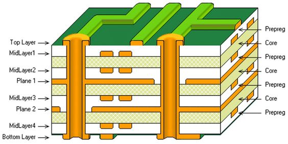
Multilayer PCBs are circuit boards that consist of three or more conductive layers stacked together. These layers are separated by insulating materials and interconnected through vias, allowing for complex and compact designs.
Advantages of Multilayer PCBs:
- Increased Density and Complexity: Multilayer PCBs enable the integration of more components and circuits within a smaller footprint, making them ideal for advanced electronic devices.
- Improved Performance: The close proximity of layers enhances signal integrity and reduces electromagnetic interference (EMI), ensuring reliable performance.
- Space-Saving Design: By stacking layers, multilayer PCBs allow for compact and lightweight designs, which are essential for modern portable devices.
These benefits make multilayer PCBs a preferred choice for industries such as telecommunications, aerospace, automotive, and consumer electronics.
Design Considerations
Building a multilayer PCB starts with meticulous planning and design. Here are the key considerations:
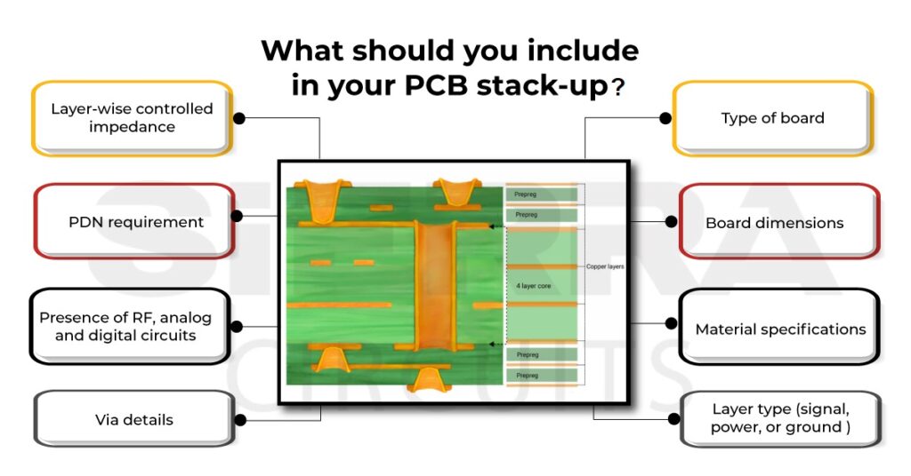
Layer Count and Stack-Up Design
The number of layers in a PCB depends on the complexity of the circuit and the application requirements. Common configurations include 4-layer, 6-layer, and even 12-layer PCBs.
Stack-up design involves arranging the layers in a way that optimizes performance. This includes selecting the right materials, such as copper thickness and dielectric materials, to meet electrical and thermal requirements.
Schematic Design
A well-structured schematic is the foundation of a successful PCB. It defines the connections between components and ensures that the design meets functional requirements.
Component placement is crucial for signal integrity and thermal management. Proper placement minimizes noise and interference while optimizing the board’s performance.
By addressing these design considerations early in the process, you can ensure a smoother manufacturing experience and a high-quality final product.
Manufacturing Process Steps
The process of building a multilayer PCB involves several precise and interconnected steps:
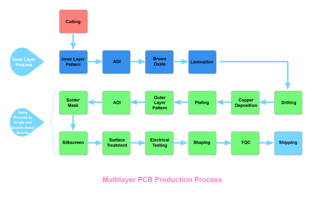
Step 1: Inner Layer Formation
The process begins with creating the inner layers. Photolithographic techniques are used to transfer the circuit pattern onto the copper-clad laminate, followed by etching to remove excess copper.
Step 2: Layer Lamination
The individual layers are aligned and bonded together using heat and pressure. This step ensures that the layers are securely laminated with insulating materials in between.
Step 3: Drilling
High-precision drilling is performed to create holes for vias, which connect the different layers electrically.
Step 4: Hole Plating
The drilled holes are plated with copper to establish electrical connections between layers. This step is critical for the functionality of the PCB.
Step 5: Outer Layer Processing
The outer layers are processed similarly to the inner layers, involving imaging, etching, and applying surface finishes to protect the copper and enhance solderability.
Step 6: Testing and Quality Control
Rigorous testing, including electrical testing and visual inspection, is conducted to ensure the PCB meets design specifications and quality standards.
Each of these steps requires precision and expertise to produce a reliable and high-performance multilayer PCB.
Advanced Techniques in Multilayer PCB Construction
To achieve optimal performance in multilayer PCBs, advanced techniques are employed:
Signal Integrity Management
Signal integrity is crucial for high-speed and high-frequency applications. Techniques such as controlled impedance, differential pair routing, and proper grounding are used to minimize crosstalk and signal loss.
Careful layer stack-up design and the use of ground planes help maintain signal quality and reduce electromagnetic interference (EMI).
Thermal Management Solutions
Effective thermal management is essential to prevent overheating and ensure the longevity of the PCB. Techniques include:
- Incorporating thermal vias to dissipate heat.
- Using copper pours and heat sinks to manage thermal loads.
- Selecting materials with high thermal conductivity for better heat dissipation.
By implementing these advanced techniques, manufacturers can produce multilayer PCBs that meet the demanding requirements of modern electronic devices.
Common Challenges in Building Multilayer PCBs
Despite their advantages, building multilayer PCBs comes with its own set of challenges. Here are some common issues and strategies to address them:
Layer Alignment and Registration
Misalignment of layers during lamination can lead to defective PCBs. To mitigate this, manufacturers use advanced alignment systems and precise registration techniques.
Manufacturing Tolerances
Tight tolerances are required for drilling, etching, and plating processes. Regular calibration of equipment and adherence to quality control standards help maintain these tolerances.
Thermal Expansion and Warping
Differences in thermal expansion rates between materials can cause warping. Using materials with similar thermal properties and optimizing the lamination process can reduce this risk.
Signal Integrity Issues
Crosstalk and EMI can degrade performance. Proper stack-up design, shielding, and routing techniques are essential to address these issues.
By understanding and addressing these challenges, manufacturers can ensure the production of reliable and high-quality multilayer PCBs.
Conclusion
Building multilayer PCBs is a complex process that requires careful planning, precise manufacturing, and advanced techniques. From understanding the basics of multilayer PCBs to addressing design considerations, manufacturing steps, and common challenges, each stage plays a critical role in ensuring the final product’s quality and performance.
By following the guidelines outlined in this article, you can gain a deeper understanding of the multilayer PCB building process and make informed decisions for your projects. Whether you are designing for high-speed applications or compact devices, the principles discussed here will help you achieve your goals.
Remember, the key to success lies in collaboration with experienced manufacturers who can bring your designs to life with precision and expertise.
Why Choose TriWin PCB for Your Multilayer PCB Needs?
At TriWin PCB, we pride ourselves on being a professional PCB manufacturer with nearly a decade of experience. Established in 2015 and located in HuiZhou City, Guangdong Province, China, our factory spans 10,000 square meters and is equipped with state-of-the-art technology. With a team of over 220 skilled experts, engineers, and technicians, we have the capability to produce up to 250,000 square meters of PCBs annually.
Our Expertise:
We specialize in a wide range of PCBs including single-sided, double-sided, multilayer PCBs as well as advanced types like HDI (High-Density Interconnect), flexible boards, metal base PCBs (aluminum base), copper base boards, and thermoelectric separation copper base boards (SinkPAD PCBs).
Our certifications—ISO9001, IATF16949, ISO14001—and UL reflect our commitment to quality manufacturing practices.
Since 2017 we have developed mature expertise in producing metal base PCBs including aluminum base boards which enhance thermal management capabilities.
Why Partner with Us?
- High-Quality Products: We use advanced manufacturing processes combined with rigorous quality control measures to deliver reliable high-performance products.
- Customer-Centric Approach: Our team works closely with clients throughout their projects ensuring tailored solutions that meet specific needs.
- Global Reach: With our extensive experience across various industries worldwide, we serve clients effectively regardless of their location.
When it comes to building multilayer PCBs, trust TriWin PCB to bring your designs to life with precision and excellence. Contact us today to discuss your project requirements or discover how we can help you achieve your goals!


